MVME2300 Series VME Processor Module
Programmer’s Reference Guide
Page
Safety Summary
Instructions
Flammability
CE Notice European Community
Limited and Restricted Rights Legend
Contents
Raven PCI Bridge Asic
Page
Page
Falcon ECC Memory Controller Chip Set
Universe VMEbus to PCI Chip
Chapter
Page
List of Figures
Page
List of Tables
Xviii
64MB ECC Dram
Model Memory Processor
16MB ECC Dram
32MB ECC Dram
Date Description of Change
Summary of Changes
Comments and Suggestions
Overview of Contents
Ctrl
Conventions Used in This Manual
Bold
Enter, Return or CR
Xxiii
Xxiv
Overview
Introduction
ECC Dram
Summary of Features
Features MVME2300 Series
Feature MVME2300
Scsa I/O
System Block Diagram
Board Description and Memory Maps
MVME2300 Series System Block Diagram
Front Panel
Functional Description
VMEbus Interface
P2 I/O
Programming Model
PCI interface
Processor Memory Maps
Processor Address Size Definition Start End
Default Processor Memory Map
Chrp Memory Map Example
Processor Chrp Memory Map
Address Register Name Register Value
Raven MPC Register Values for Chrp Memory Map
Bfff Ffff
Processor Prep Memory Map
Prep Memory Map Example
Raven MPC Register Values for Prep Memory Map
PCI Configuration Access
PCI Address Size Definition Start End
Default PCI Memory Map
PCI Memory Maps
PCI Chrp Memory Map
FC03 Ffff
Universe PCI Register Values for Chrp Memory Map
Configuration Register Value Address Offset Register Name
Raven PCI Register Values for Chrp Memory Map
10. PCI Prep Memory Map
PCI Prep Memory Map
3AFE Ffff
38FF Ffff
39FE Ffff
39FF Ffff
11. Raven PCI Register Values for Prep Memory Map
12. Universe PCI Register Values for Prep Memory Map
VMEbus Master Map
VMEbus Mapping
VMEbus Slave Map
VMEbus Slave Mapping
VSI0TO
VSI0CTL
VSI0BS
VSI0BD
15. System Register Summary
VMEbus Address Size Chrp Map Prep Map Range Mode
Falcon-Controlled System Registers
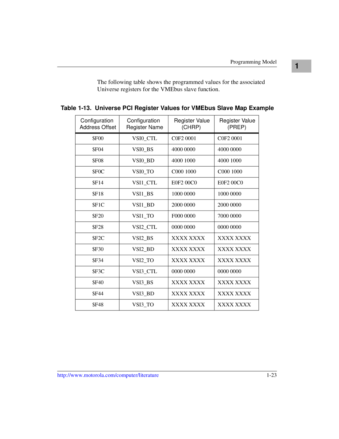
14. VMEbus Slave Map Example
Sysclk Value System Clock Speed PCI Clock Speed
System Configuration Register Syscr
System Configuration Register $FEF80400
$FD
P0/1STAT Value Processor 0/1 Present External In-line Cache
MSIZE01 Total Memory On Board
Memory Configuration Register Memcr
Memory Configuration Register $FEF80404
MSIZE01
L2TYPE03
MSPD01
RA/BTYP02
PLL Value Size
L2PLL03
FLSHP02
System External Cache Control Register Sxccr
CPU Control Register $FEF88300
Processor 0 External Cache Control Register P0XCCR
Processor 1 External Cache Control Register P1XCCR
CPU Control Register
Uart
Access Registers
ISA Local Resource Bus
W83C553 PIB Registers
General-Purpose Readable Jumpers
NVRAM/RTC and Watchdog Timer Registers
PCI I/O Address Function
Module Configuration and Status Registers
17. M48T59/559 Access Registers
18. Module Configuration and Status Registers
SD7 SD6 SD5 SD4 SD3 SD2 SD1 SD0
CPU Configuration Register
Old CPU Configuration Register $FE000800
Cputype
Pcixp PMC2P PMC1P Vmep Lanp
Base Module Feature Register
Base Module Feature Register Offset $0802
Basetype
Base Module Status Register Bmsr
Basetype
Base Module Status Register Offset $0803
SD9 SD8 SD7 SD6 SD5 SD4 SD3 SD2 SD1 SD0
VME Registers
Seven-Segment Display Register
Segment Display Register Offset $08C0
SETSIG0
19. VME Registers
LM/SIG Control Register
SETSIG1
LM/SIG Status Register
Board Description and Memory Maps
Location Monitor Lower Base Address Register Offset $1003
Location Monitor Upper Base Address Register
Location Monitor Lower Base Address Register
Location Monitor Upper Base Address Register Offset $1002
Semaphore Register 2 Offset $1005
Semaphore Register
Semaphore Register 1 Offset $1004
SEM1
Emulated Z8536 Registers
Emulated Z8536 CIO Registers and Port Pins
20. Emulated Z8536 Access Registers
VME Geographical Address Register Vgar
21. Z8536 CIO Port Pin Assignments
Z8536 CIO Port Pins
Port Signal Direction Descriptions Pin Name
PC3 BASETYP1
ISA DMA Channels
PC2 BASETYP0
Page
Function Features
Features
Features of the Raven Asic
Block Diagram
Raven Block Diagram
MPC Address Mapping
MPC Bus Interface
MPC-to-PCI Address Decoding
MPC Slave
MPC to PCI Address Translation
MPC Transfer Type Transaction Encoding
Command Types MPC Slave Response
MPC Master
MPC Write Posting
MPC Transfer Type MPC Transfer Size TT0-TT4
PCI Command Code
MPC Transfer Types
MPC Arbiter
MPC Bus Timer
PCI Address Mapping
Configuration Registers
PCI to MPC Address Decoding
MPC Bus Address Space
Decoder Priority
RavenMPIC Control Registers
PCI Slave
Addressing
Command Types
Command Types PCI Slave Response
Command Type Slave Response?
Fast Back-to-Back Transactions
Exclusive Access
Device Selection
Target-Initiated Termination
PCI Master
Parity
Cache Support
PCI Write Posting
Transfer Type
PCI Master Command Codes
PCI Command
Entity Addressed
Master Initiated Termination
Combining, Merging, and Collapsing
Address/Data Stepping
Arbitration
Arbitration Latency
PCI Cycle Type
Generating PCI Cycles
Generating PCI Memory and I/O Cycles
PCI Spread I/O Address Translation
Generating PCI Configuration Cycles
Functional Description
Device Number Address Bit
Generating PCI Special Cycles
Generating PCI Interrupt Acknowledge Cycles
When MPC Devices are Big-Endian
Endian Conversion
Big- to Little-Endian Data Swap
Data Address Length Bytes Modification
When MPC Devices are Little-Endian
Raven Registers and Endian Mode
Address Modification for Little-Endian Transfers
Error Handling
Perr
Error Status Error Address Attributes
Transaction Ordering
SMA
MPC Registers
Raven Registers
Raven MPC Register Map
Devid
Vendor ID/Device ID Registers
Venid
Revision ID. Identifies the Raven revision level. This
General Control-Status/Feature Registers
Revision ID Register
Revid
Mpic
Flbrd
Bhog
Marb
Current MPC Data Bus Master
MIDx
Feat
MPC Arbiter Control Register
Prescaler Adjust Register
Operation Reset $00
Operation Reset $00 $B4
Matom
MPC Error Enable Register
Perri
Smam
Rtam
Matoi
Mato
MPC Error Status Register
OVF
RTA
Writing it to a 0 has no effect. When the Smam bit
SMA
PCI transaction. The bit may be cleared by writing it to a
TTx
MPC Error Attribute Register Merat
Which originated the transfer in which the error occurred
Register
Designates a selected byte
Address $FEFF0030 Bit Name
Operation Reset $0000
PCI Interrupt Acknowledge Register
Piack
MPC Slave Address 3 Register
Operation Reset $8000 $8080
Start
END
WEN
MPC Slave Offset/Attribute 0,1 and 2 Registers
MSOFFx
REN
MSOFF3
Wpen
IOM
PCI Registers
Cycles. When clear, the corresponding MPC slave will
$8C
Raven PCI Configuration Register Map
$0C
$18 $7F
Offset $00 Bit Name
Operation Reset $4801 $1057
Raven PCI I/O Register Map
$CF8
PCI Command/ Status Registers
Rcvta
Dpar
Seltim
Sigta
Space
Revision ID/ Class Code Registers
Class
Base Register
PRE
RES
Ioba
IO/MEM
Be compared with the upper 16 bits of the incoming PCI
To access MPC bus resources. The value of this field will
PCI Slave Address 0,1,2 and 3 Registers
GBL
PCI Slave Attribute/ Offset 0,1,2 and 3 Registers
INV
Transfer type code which specifies the current transaction
Conceptual perspective from the PCI bus
Configaddress Register
Perspective from the MPC bus in Big-Endian mode
DEV
Perspective from the MPC bus in Little-Endian mode
REG
FUN
BUS
EN Enable
Configdata Register
Data ‘B’ Data ‘C’ Data ‘D’ Operation Reset
Data ‘D’ Data ‘C’ Data ‘B’ Data ‘A’ Operation Reset
Architecture
Features
Raven Interrupt Controller
Processor’s Current Task Priority
Readability of CSR
Interrupt Source Priority
Compatibility
Nesting of Interrupt Events
Spurious Vector Generation
Interprocessor Interrupts IPI
Timers
Raven-Detected Errors
Interrupt Delivery Modes
Raven Interrupt Controller
Block Diagram Description
Interrupt Selector is
Program-Visible Registers
Interrupt Pending Register IPR
Interrupt Router
In-Service Register ISR
Interrupt Request Register IRR
Raven PCI Bridge Asic
Off
Mpic Registers
RavenMPIC Registers
10. RavenMPIC Register Map
$011E0
$010E0
$010F0
$100F0
$100E0
$101F0
$101E0
VID
Feature Reporting Register
Ncpu
Offset $01020 Bit Name
Global Configuration Register
Processor Init Register
Processor 1. Writing a 1 to P1 will assert the Soft Reset
Vendor Identification Register
STP
Prior
IPI Vector/Priority Registers
Mask
ACT
Offset $010E0 Bit Name
Spurious Vector Register
Interrupt Acknowledge register is read during a spurious
Vector fetch
Timer Base Count Registers
Timer Current Count Registers
Bit transitions from a 1 to a 0, the value is copied into
Count Inhibit. Setting this bit to 1 inhibits counting for
This timer. Setting the bit to 0 allows counting to proceed
Base Count. This field contains the 31-bit count for this
Timer Destination Registers
Sense
Setting this bit to a 0 enables active low or negative edge
External Source Vector/Priority Registers
POL
External Source Destination Registers
Offset $10200 Bit Name
Raven-Detected Errors Vector/Priority Register
Offset $10210 Bit Name
Raven-Detected Errors Destination Register
Offset Processor $20080 $21080 Bit Name
End Of Interrupt. There is one EOI register per
Zero is assumed. Writing to this register signals the end
Interrupt Acknowledge Registers
End-of-Interrupt Registers
Programming Notes
External Interrupt Service
Reset State
Interprocessor Interrupts
Dynamically Changing I/O Interrupt Configuration
Current Task Priority Level
EOI Register
Interrupt Acknowledge Register
Mode
Architectural Notes
Page
Dram
Features of the Falcon Chip Set
Falcon Pair Used with Dram in a System
Block Diagrams
Falcon Internal Data Paths Simplified
Overall Dram Connections
Four-beat Reads/Writes
Bit Ordering Convention
Performance
Dram Speeds
Single-beat Reads/Writes
Beat
PowerPC 60x Bus to Dram Access Timing 70ns Page Devices
Clock Periods Required For Total Access Type
2nd 3rd 4th
2nd 3rd 4th Clocks Beat
PowerPC 60x Bus to Dram Access Timing 60ns Page Devices
PowerPC Bus to Dram Access Timing 50ns Hyper Devices
ROM/Flash Speeds
Cache Coherency
PowerPC 60x Bus Interface
Responding to Address Transfers
Completing Data Transfers
Cycle Types
Cache Coherency Restrictions
L2 Cache Support
Single-Bit
Error Reporting
ROM/Flash Interface
Error Logging
Dram Tester
Functional Description
$XXFFFFFB $7FFFFF
$XXFFFFF8 $7FFFFC
$XXFFFFF9 $7FFFFD
$XXFFFFFA $7FFFFE
$X3FFFFF3 $7FFFFE
$X3FFFFF0 $7FFFFE
$X3FFFFF1 $7FFFFE
$X3FFFFF2 $7FFFFE
Blocks a and/or B Present, Blocks C and D Not Present
Refresh/Scrub
Blocks a and/or B Present, Blocks C and/or D Present
Dram Arbitration
Chip Defaults
CSR Architecture
CSR Accesses
External Register Set
Data Path for Reads from the Falcon Internal CSRs
Data Path for Writes to the Falcon Internal CSRs
Memory Map for Byte Reads to CSR
1906
Memory Map for 4-Byte Reads to CSR
Detailed Register Bit Descriptions
Register Summary
10. Register Summary
Test D3 Lower 32 Bits
Programming Model
Address $FEF80000 Bit Name
Vendor/Device Register
Read Zero Read only
Revision ID/ General Control Register
Ram spd0, ram spd1 Dram Speed Dram Type
Ram spd0,ram spd1
11. ram spd1,ram spd0 and Dram Type
Ram a/b/c/d siz0-2
Dram Attributes Register
Ram a/b/c/d en
SIMM/DIMM
BlockA/B/C/D Configurations
Ram a/b/c/d Block Size Devices Used Technology Comments
0MB
CLK Frequency
Dram Base Register
RAM A/B/C/D Base
CLK Frequency Register
Read Zero
ECC Control Register
Refdis
Rwcb
11707.00
Falcon ECC Memory Controller Chip Set
Mcken
Tien
Sien
Mien
Elog
Embt
Esen
Address $FEF80038 Bit Name
Error Address Register
13. rtest Encodings
Rtest0,rtest1,rtest2 Test Mode selected
Address $FEF80048 Bit Name
Refresh/Scrub Address Register
1Mbyte of Block a also appears at $FFF00000
ROM a Base
1MB
14. ROM Block a Size Encoding
15. romarv and rombrv Encoding
Rom a siz Block Size
Cycle Transfer Alignment Romx64 Romxwe Falcon Response
16. Read/Write to ROM/Flash
1Mbyte of Block B also appears at $FFF00000
ROM B Base/Size Register
ROM B Base
Rom b siz Block Size
17. ROM Block B Size Encoding
Has been programmed properly. Notice that CTR32 is
Dram Tester Control Registers
Bit Counter
CTR32 is a 32-bit, free-running counter that increments
Address $FEF80500 Bit Name
Power-Up Reset Status Register
Address $FEF80400 Bit Name
Address $FEF88000 $FEF8FFF8 Bit Name
External Register Set
Writing to the Control Registers
Parity Checking on the PowerPC Bus
Software Considerations
Programming ROM/Flash Devices
Sizing Dram
Software Considerations
ROW
19. PowerPC 60x Address to Dram Address Mappings
18. Sizing Addresses
1024MB 256MB 128MB 64MB 32MB 16MB
Bit Syndrome
20. Syndrome Codes Ordered by Bit in Error
ECC Codes
20. Syndrome Codes Ordered by Bit in Error
$AF $CF $EF
21. Single-Bit Errors Ordered by Syndrome Code
Data Paths
10. PowerPC Data to Dram Data Correspondence
22. PowerPC Data to Dram Data Mapping
Page
Universe VMEbus to PCI Chip
− BLT, ADOH, RMW, Lock
Features of the Universe Asic
Block Diagram
Universe as VMEbus Slave
Architectural Diagram for the Universe
Universe as VMEbus Master
PCI Bus Interface
Universe as PCI Slave Universe as PCI Master
Interrupter
VMEbus Interrupt Handling
DMA Controller
Universe Control and Status Registers Ucsr
Ucsr Access Mechanisms Universe Register Map
Offset Register Name
LSI3BS
LSI2BS
LSI2BD
LSI2TO
Linten
Dcpp
Dgcs
Dllue
VSI2BS
VSI0BD F0C
VSI1BS F1C
VSI2CTL F2C
Description
Universe Chip Problems after PCI Reset
Method
Workarounds
Examples
Example 1 MVME2600 Series Board Exhibits PCI Reset Problem
Example 2 MVME3600 Series Board Acts Differently
Run the init code and the LSI0 registers become
Example 3 Universe Chip is Checked at Tundra
Universe VMEbus to PCI Chip
PIB
PCI Arbitration
PCI Arbitration Assignments
Pci Bus Request PCI Masters
MVME2300 Series Interrupt Architecture
Interrupt Handling
Level
RavenMPIC
RavenMPIC Interrupt Assignments
Edge Polarity Interrupt Source
IRQ15
Interrupts
IRQ14
PIB Interrupt Handler Block Diagram
Edge
PIB PCI/ISA Interrupt Assignments
ISA DMA Channels
Exceptions
Sources of Reset
Reset switch
Devices Affected
Soft Reset
Reset Sources and Devices Affected
Sources of Reset
Cause Action
Error Notification and Handling
Error Notification and Handling
Big-Endian Mode
Endian Issues
Little-Endian Mode
PCI/Ethernet
Processor/Memory Domain
Role of the Raven Asic
PCI Domain
PCI-Graphics
Role of the Universe Asic
VMEbus Domain
ROM/Flash Initialization
ROM/Flash Bank Default
Default Mapping for FFF00000-FFFFFFFF
Page
Document Title Publication Number
Motorola Computer Group Documents
Document Title and Source Publication Number
Manufacturers’ Documents
EK-DE500-OM
MPCFPE/AD
IEC 821 BUS
Related Specifications
ANSI/IEEE
TIA/EIA-232
MPR-PPC-RPU-02
Isbn
Page
Glossary
O S S a R Y
Enhanced Integrated Drive Electronics. An improved version
PCI. Used in the reference platform specification. IBM
IBM
Computers developed by the IBM Corporation. PowerPC is
Signal Computing System Architecture. a hardware model for
See 10base-2
Page
Index
PCI 1-13 processor
IN-3
PCI
MPC
IN-5
Configaddress 2-56CONFIGDATA
IN-7
IN-8