TMS320 SECOND-GENERATION
DEVICES
SPRS010B Ð MAY 1987 Ð REVISED NOVEMBER 1990
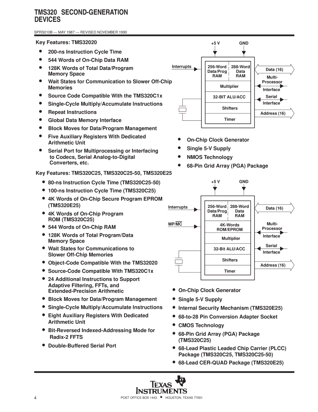
Key Features: TMS32020 | +5 V | GND |
•
•544 Words of
• 128K Words of Total Data/Program | Interrupts | Data (16) | |||
| Data/Prog | Data | |||
Memory Space |
|
| |||
| RAM | RAM | Multi- | ||
• Wait States for Communication to Slower | |||||
|
| ||||
Multiplier | Processor | ||||
Memories |
|
| |||
| Interface | ||||
• Source Code Compatible With the TMS320C1x |
|
|
| ||
| Serial | ||||
• |
|
|
|
| |
| Shifters | Interface | |||
• Repeat Instructions |
|
| |||
|
|
| Address (16) | ||
• Global Data Memory Interface |
| Timer |
| ||
• Block Moves for Data/Program Management |
|
|
|
|
| |
|
|
|
|
| ||
|
|
|
|
| ||
• Five Auxiliary Registers With Dedicated | • | |||||
Arithmetic Unit | ||||||
• Single | ||||||
• Serial Port for Multiprocessing or Interfacing | ||||||
• NMOS Technology | ||||||
to Codecs, Serial | ||||||
Converters, etc. | • | |||||
| ||||||
Key Features: TMS320C25, |
|
|
|
|
| |
• |
• |
• 4K Words of |
(TMS320E25) |
• 4K Words of |
ROM (TMS320C25) |
• 544 Words of |
• 128K Words of Total Program/Data |
Memory Space |
• Wait States for Communications to |
Slower |
• |
• |
• 24 Additional Instructions to Support |
Interrupts
MP/MC
+5 V | GND |
Data/Prog Data
RAM RAM
ROM/EPROM
Multiplier
Shifters
Timer
Data (16)
Multi-
Processor
Interface
Serial
Interface
Address (16)
Adaptive Filtering, FFTs, and |
|
• Block Moves for Data/Program Management |
• |
• Eight Auxiliary Registers With Dedicated |
Arithmetic Unit |
• |
|
• |
•
•Single
•Internal Security Mechanism (TMS320E25)
•
•CMOS Technology
•
•
•
4 | POST OFFICE BOX 1443 • HOUSTON, TEXAS 77001 |