Description
TMS320 SECOND-GENERATION Digital Signal Processors
Function PIN
Signals Definition
PGA and PLCC/CER-QUAD PIN Assignments
Introduction
Wait States for Communication to Slower Off-Chip
Key Features TMS32020
Bit-Reversed Indexed-Addressing Mode for
Memory Space
Type
Architecture
TMS320 Second-Generation Device Overview
Package
SECOND-GENERATION Devices
Functional block diagram TMS320C2x
Memory control
Timer
Scaling shifter
16 ⋅ 16-bit parallel multiplier
Memory Maps
TMS320 SECOND-GENERATION Devices
Multiprocessing
Interrupts and subroutines
External interface
Addressing modes
Repeat feature
Instruction set
Instruction set summary
Instruction Symbols
Symbol Definition
TMS320C25 Instruction Set Summary
ZAC
SUBT²
XOR
XORK²
LTP ²
Apac
LPH ²
LTA
Data Memory Operations Mnemonic Description Words
TMS320C25 Instruction Set Summary concluded
TMS32020 Product Notification
TMS32020
Development support
Hardware Tools Part Number
TMS320 Second-Generation Software and Hardware Support
Software Tools Part Number
Documentation support
Specification overview
Parameter Test Conditions MIN TYP§ MAX Unit
Recommended operating conditions
MIN NOM MAX Unit
External clock option
Clock Characteristics and Timing
Internal clock option
Test Load Circuit
Parameter MIN TYP MAX Unit
Memory and Peripheral Interface Timing
Hold Holda
RS, INT, BIO, and XF Timing
Hold Timing
Serial Port Timing
TMS320C25GBA
INT Clkin / Clkx / Clkr
MP/MC IOH
Parameter Test Conditions MIN TYP MAX Unit
Clkin
External Clock Option
VOH Min
TdC1L-AL Low after CLKOUT1 low
Serial Port Timing
IPP1
Eprom Programming
See Notes 14
VPP
MP/MC VIL
INT0 INT2 VIH
CLKIN, CLKX, Clkr
CLKOUT1, CLKOUT2
Internal Clock Option External clock option
Fcrystal
TdC1-S From Clkout if Is present
TsuIN Setup before CLKOUT1 high
MIN TYP MAX
Contrast Summary of Electrical Specifications
Clock characteristics and timing
Parameter
Serial port timing
Memory and peripheral interface timing
RS, INT, BIO, and XF timing
Hold timing
Clock timing
Timing Diagrams
Ready
Memory read timing
BR, PS, D S
CLKOUT1 CLKOUT2 Strb
Memory write timing
MSC
One wait-state memory access timing
Iack
Reset timing
Interrupt timing TMS320C25
Interrupt timing TMS32020
Serial port transmit timing
Serial port receive timing
External flag timing
BIO timing
PC = N PC = N +
Execute
Hold timing part a
Hold
Holda
Holda Fetch
Hold timing part B
CLKOUT1 CLKOUT2
Fetch Execute
Or is D15-D0 TdHH-AH
TMS320C25FNL Plcc reflow soldering precautions
Typical Supply Current Characteristics for TMS320C25
Parameter MAX Unit
Mechanical Data
Pin GB grid array ceramic package TMS32020, TMS320C25
Advance
Jedec NO. Outline Terminals MIN MAX
Fast programming and verification
Programming the TMS320E25 Eprom cell
EPT VPP
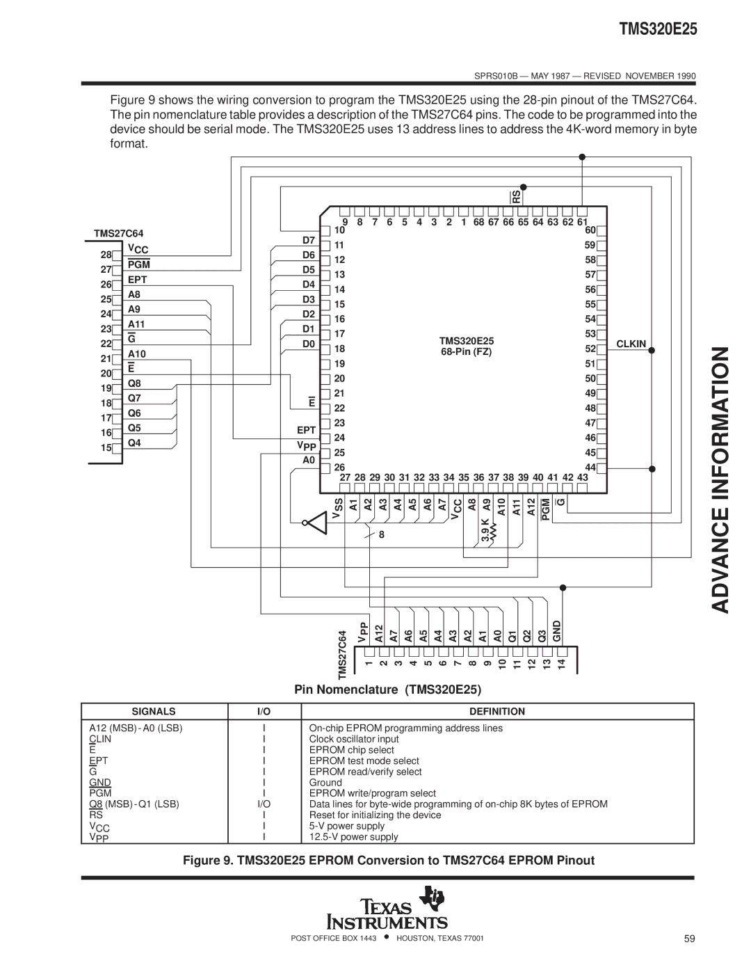
Pin Nomenclature TMS320E25
VCC
EPT
Erasure
TMS320E25 Programming Mode Levels
Signal
Program Read Output Name ² PIN Verify Inhibit Disable
Program verify
Fast Programming Flowchart
ROM protection and verification
Output disable
Read
VSS Clkin EPT VPP
TMS320E25 Protect and Verify Eprom Mode Levels
Eprom protect
VIH VIL PGM VPP VCC
Rbit
Eprom
VCC VIH VIL PGM VIH/VOH HI-Z VIL/VOL VPP EPT VSS
VIH VIL VPP VCC
TMS320 SECOND-GENERATION
NIL
Other Qualified Versions of TMS320C25
Packaging Information
Important Notice