•
•544 Words of
•4K Words of
•4K Words of
•128K Words of Data/Program Space
•
•16 ⋅
•Block Moves for Data/Program Management
•Repeat Instructions for Efficient Use of Program Space
•Serial Port for Direct Codec Interface
•Synchronization Input for Synchronous Multiprocessor Configurations
•Wait States for Communication to Slow
•
•Single
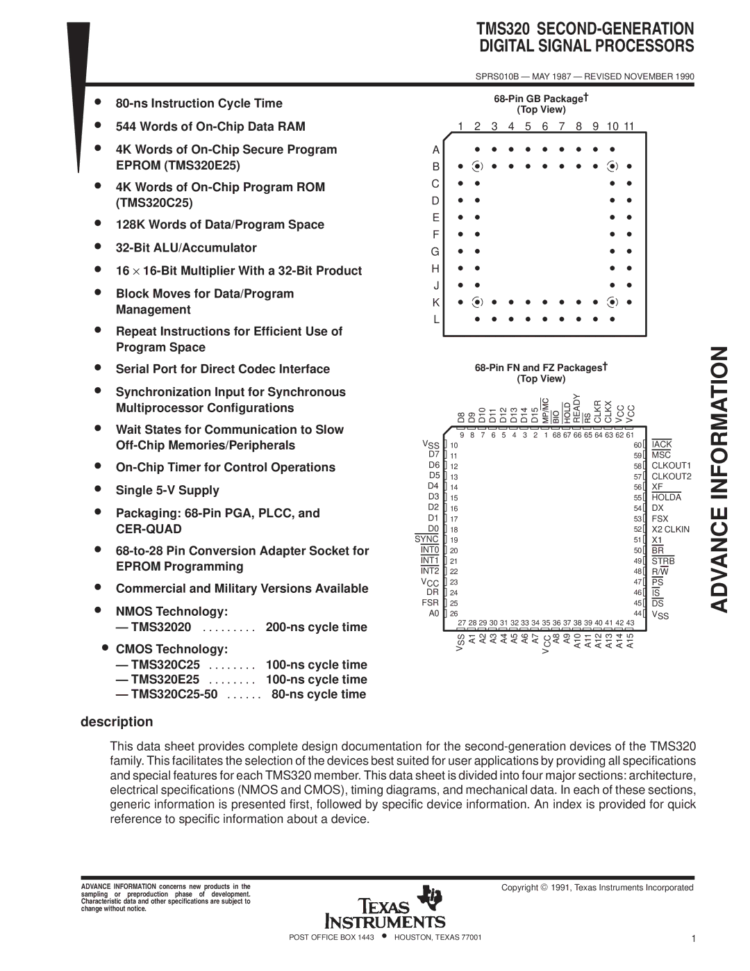
•Packaging:
CER-QUAD
•
•Commercial and Military Versions Available
•NMOS Technology:
ÐTMS32020 . . . . . . . . .
•CMOS Technology:
ÐTMS320C25 . . . . . . . .
ÐTMS320E25 . . . . . . . .
Ð
TMS320 SECOND-GENERATION DIGITAL SIGNAL PROCESSORS
SPRS010B Ð MAY 1987 Ð REVISED NOVEMBER 1990
(Top View)
1 2 3 4 5 6 7 8 9 10 11
A
B
C
D
E
F
G
H
J
K
L
68-Pin FN and FZ Packages²
(Top View)
|
|
|
|
| D8 |
| D9 |
| D10 |
| D11 |
| D12 |
| D13 |
| D14 |
| D15 |
|
|
|
|
|
|
| READY |
|
|
| CLKR CLKX |
| V | V |
|
|
|
|
|
|
| ||||
|
|
|
|
|
|
|
|
|
|
|
|
|
|
|
|
|
|
|
|
|
|
|
|
|
|
|
|
|
| ||||||||||||||||
|
|
|
|
|
|
|
|
|
|
|
|
|
|
|
|
|
|
|
|
|
|
|
|
|
|
|
|
|
|
|
|
|
|
| CC | CC |
|
|
|
|
|
|
| ||
|
|
|
|
|
|
|
|
|
|
|
|
|
|
|
|
|
|
|
|
|
|
|
|
|
|
|
|
|
|
|
|
|
|
|
|
|
|
|
|
|
| ||||
|
|
|
|
|
|
|
|
|
|
|
|
|
|
|
|
|
|
|
|
|
|
|
|
|
|
|
|
|
|
|
|
|
|
|
|
|
|
|
|
|
|
|
|
|
|
|
|
|
|
|
|
|
|
|
|
|
|
|
|
|
|
|
|
|
|
|
|
|
|
|
|
|
|
|
|
|
|
|
|
|
|
|
|
|
|
|
|
|
|
|
|
| VSS | 9 | 8 | 7 | 6 | 5 | 4 | 3 | 2 | 1 |
| 68 67 66 65 64 63 62 61 |
|
|
|
|
|
|
| ||||||||||||||||||||||||||
|
| 10 |
|
|
|
|
|
|
|
|
|
|
|
|
|
|
|
|
|
|
|
|
|
|
|
|
|
|
|
|
|
|
| 60 |
|
| IACK |
|
|
| |||||
|
|
|
|
|
|
|
|
|
|
|
|
|
|
|
|
|
|
|
|
|
|
|
|
|
|
|
|
|
|
|
|
| |||||||||||||
| D7 |
| 11 |
|
|
|
|
|
|
|
|
|
|
|
|
|
|
|
|
|
|
|
|
|
|
|
|
|
|
|
|
|
|
| 59 |
| MSC | ||||||||
| D6 |
| 12 |
|
|
|
|
|
|
|
|
|
|
|
|
|
|
|
|
|
|
|
|
|
|
|
|
|
|
|
|
|
|
| 58 |
| CLKOUT1 | ||||||||
| D5 |
| 13 |
|
|
|
|
|
|
|
|
|
|
|
|
|
|
|
|
|
|
|
|
|
|
|
|
|
|
|
|
|
|
| 57 |
| CLKOUT2 | ||||||||
| D4 |
| 14 |
|
|
|
|
|
|
|
|
|
|
|
|
|
|
|
|
|
|
|
|
|
|
|
|
|
|
|
|
|
|
| 56 |
| XF | ||||||||
| D3 |
| 15 |
|
|
|
|
|
|
|
|
|
|
|
|
|
|
|
|
|
|
|
|
|
|
|
|
|
|
|
|
|
|
| 55 |
|
| HOLDA |
| ||||||
| D2 |
| 16 |
|
|
|
|
|
|
|
|
|
|
|
|
|
|
|
|
|
|
|
|
|
|
|
|
|
|
|
|
|
|
| 54 |
| DX | ||||||||
| D1 |
| 17 |
|
|
|
|
|
|
|
|
|
|
|
|
|
|
|
|
|
|
|
|
|
|
|
|
|
|
|
|
|
|
| 53 |
| FSX | ||||||||
| D0 |
| 18 |
|
|
|
|
|
|
|
|
|
|
|
|
|
|
|
|
|
|
|
|
|
|
|
|
|
|
|
|
|
|
| 52 |
| X2 CLKIN | ||||||||
| SYNC |
|
| 19 |
|
|
|
|
|
|
|
|
|
|
|
|
|
|
|
|
|
|
|
|
|
|
|
|
|
|
|
|
|
|
| 51 |
| X1 | |||||||
| INT0 |
|
|
|
|
|
|
|
|
|
|
|
|
|
|
|
|
|
|
|
|
|
|
|
|
|
|
|
|
|
|
|
| 50 |
| BR | |||||||||
| 20 |
|
|
|
|
|
|
|
|
|
|
|
|
|
|
|
|
|
|
|
|
|
|
|
|
|
|
|
|
|
|
|
| ||||||||||||
| INT1 |
| 21 |
|
|
|
|
|
|
|
|
|
|
|
|
|
|
|
|
|
|
|
|
|
|
|
|
|
|
|
|
|
|
| 49 |
|
| STRB |
| ||||||
| INT2 |
| 22 |
|
|
|
|
|
|
|
|
|
|
|
|
|
|
|
|
|
|
|
|
|
|
|
|
|
|
|
|
|
|
| 48 |
| R/W | ||||||||
| VCC |
|
|
|
|
|
|
|
|
|
|
|
|
|
|
|
|
|
|
|
|
|
|
|
|
|
|
|
|
|
|
|
| 47 |
| PS | |||||||||
| 23 |
|
|
|
|
|
|
|
|
|
|
|
|
|
|
|
|
|
|
|
|
|
|
|
|
|
|
|
|
|
|
|
| ||||||||||||
|
|
|
|
|
|
|
|
|
|
|
|
|
|
|
|
|
|
|
|
|
|
|
|
|
|
|
|
|
|
|
|
|
|
| |||||||||||
| DR |
| 24 |
|
|
|
|
|
|
|
|
|
|
|
|
|
|
|
|
|
|
|
|
|
|
|
|
|
|
|
|
|
|
| 46 |
| IS | ||||||||
| FSR |
| 25 |
|
|
|
|
|
|
|
|
|
|
|
|
|
|
|
|
|
|
|
|
|
|
|
|
|
|
|
|
|
|
| 45 |
|
| DS |
| ||||||
| A0 |
|
|
|
|
|
|
|
|
|
|
|
|
|
|
|
|
|
|
|
|
|
|
|
|
|
|
|
|
|
|
|
| 44 |
| VSS | |||||||||
| 26 |
|
|
|
|
|
|
|
|
|
|
|
|
|
|
|
|
|
|
|
|
|
|
|
|
|
|
|
|
|
|
|
| ||||||||||||
|
|
|
| 27 28 29 30 31 32 33 34 35 36 37 38 39 40 41 42 43 |
|
|
|
|
|
|
| ||||||||||||||||||||||||||||||||||
|
|
|
|
|
|
|
|
|
|
|
|
|
|
|
|
|
|
|
|
|
|
|
|
|
|
|
|
|
|
|
|
|
|
|
|
|
|
|
|
|
|
|
|
|
|
|
|
|
| V |
| A1 |
| A2 |
| A3 |
| A4 |
| A5 |
| A6 |
| A7 |
| V | A8 A9 A10 |
| A11 A12 A13 |
| A14 | A15 |
|
|
|
|
|
|
| ||||||||||||
|
|
|
|
| SS |
|
|
|
|
|
|
|
|
|
|
|
|
|
|
| CC |
|
|
|
|
|
|
|
|
|
|
|
|
|
|
|
|
|
|
|
|
|
|
| |
ADVANCE INFORMATION
description
This data sheet provides complete design documentation for the
ADVANCE INFORMATION concerns new products in the sampling or preproduction phase of development. Characteristic data and other specifications are subject to change without notice.
Copyright 1991, Texas Instruments Incorporated
POST OFFICE BOX 1443 • HOUSTON, TEXAS 77001 | 1 |