TMS320 SECOND-GENERATION
DEVICES
SPRS010B Ð MAY 1987 Ð REVISED NOVEMBER 1990
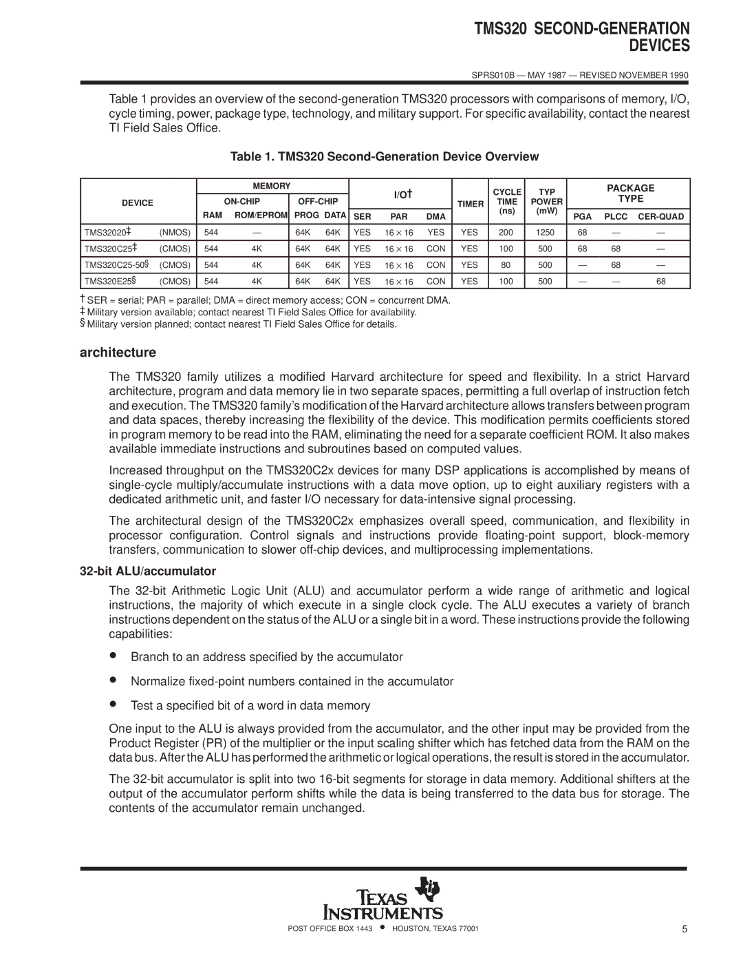
Table 1 provides an overview of the
Table 1. TMS320 Second-Generation Device Overview
|
|
| MEMORY |
|
|
| I/O² |
|
| CYCLE | TYP |
| PACKAGE | ||
DEVICE |
|
|
|
|
|
| TIMER | TIME | POWER |
| TYPE | ||||
|
|
|
|
|
|
|
|
| |||||||
|
| RAM | ROM/EPROM | PROG DATA |
|
|
|
| (ns) | (mW) |
|
|
| ||
|
| SER | PAR | DMA |
| PGA | PLCC |
| |||||||
|
|
|
|
| |||||||||||
|
|
|
|
|
|
|
|
|
|
|
|
|
|
|
|
TMS32020³ | (NMOS) | 544 | Ð |
| 64K | 64K | YES | 16 ⋅ 16 | YES | YES | 200 | 1250 | 68 | Ð | Ð |
TMS320C25³ | (CMOS) | 544 | 4K |
| 64K | 64K | YES | 16 ⋅ 16 | CON | YES | 100 | 500 | 68 | 68 | Ð |
(CMOS) | 544 | 4K |
| 64K | 64K | YES | 16 ⋅ 16 | CON | YES | 80 | 500 | Ð | 68 | Ð | |
TMS320E25§ | (CMOS) | 544 | 4K |
| 64K | 64K | YES | 16 ⋅ 16 | CON | YES | 100 | 500 | Ð | Ð | 68 |
²SER = serial; PAR = parallel; DMA = direct memory access; CON = concurrent DMA. ³ Military version available; contact nearest TI Field Sales Office for availability.
§ Military version planned; contact nearest TI Field Sales Office for details.
architecture
The TMS320 family utilizes a modified Harvard architecture for speed and flexibility. In a strict Harvard architecture, program and data memory lie in two separate spaces, permitting a full overlap of instruction fetch and execution. The TMS320 family's modification of the Harvard architecture allows transfers between program and data spaces, thereby increasing the flexibility of the device. This modification permits coefficients stored in program memory to be read into the RAM, eliminating the need for a separate coefficient ROM. It also makes available immediate instructions and subroutines based on computed values.
Increased throughput on the TMS320C2x devices for many DSP applications is accomplished by means of
The architectural design of the TMS320C2x emphasizes overall speed, communication, and flexibility in processor configuration. Control signals and instructions provide
The
•
•
•
Branch to an address specified by the accumulator
Normalize
Test a specified bit of a word in data memory
One input to the ALU is always provided from the accumulator, and the other input may be provided from the Product Register (PR) of the multiplier or the input scaling shifter which has fetched data from the RAM on the data bus. After the ALU has performed the arithmetic or logical operations, the result is stored in the accumulator.
The
POST OFFICE BOX 1443 • HOUSTON, TEXAS 77001 | 5 |