www.ti.com
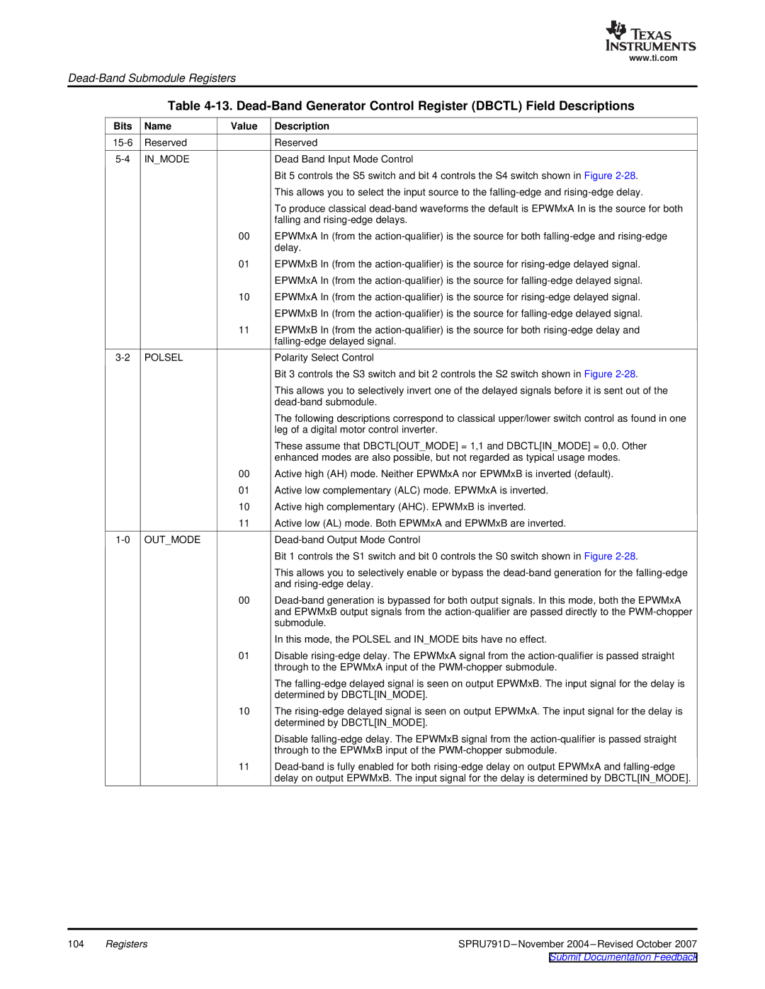
Table
Bits | Name | Value | Description |
Reserved |
| Reserved | |
IN_MODE |
| Dead Band Input Mode Control | |
|
|
| Bit 5 controls the S5 switch and bit 4 controls the S4 switch shown in Figure |
|
|
| This allows you to select the input source to the |
|
|
| To produce classical |
|
|
| falling and |
|
| 00 | EPWMxA In (from the |
|
|
| delay. |
|
| 01 | EPWMxB In (from the |
|
|
| EPWMxA In (from the |
|
| 10 | EPWMxA In (from the |
|
|
| EPWMxB In (from the |
|
| 11 | EPWMxB In (from the |
|
|
| |
POLSEL |
| Polarity Select Control | |
|
|
| Bit 3 controls the S3 switch and bit 2 controls the S2 switch shown in Figure |
|
|
| This allows you to selectively invert one of the delayed signals before it is sent out of the |
|
|
| |
|
|
| The following descriptions correspond to classical upper/lower switch control as found in one |
|
|
| leg of a digital motor control inverter. |
|
|
| These assume that DBCTL[OUT_MODE] = 1,1 and DBCTL[IN_MODE] = 0,0. Other |
|
|
| enhanced modes are also possible, but not regarded as typical usage modes. |
|
| 00 | Active high (AH) mode. Neither EPWMxA nor EPWMxB is inverted (default). |
|
| 01 | Active low complementary (ALC) mode. EPWMxA is inverted. |
|
| 10 | Active high complementary (AHC). EPWMxB is inverted. |
|
| 11 | Active low (AL) mode. Both EPWMxA and EPWMxB are inverted. |
OUT_MODE |
| ||
|
|
| Bit 1 controls the S1 switch and bit 0 controls the S0 switch shown in Figure |
|
|
| This allows you to selectively enable or bypass the |
|
|
| and |
|
| 00 | |
|
|
| and EPWMxB output signals from the |
|
|
| submodule. |
|
|
| In this mode, the POLSEL and IN_MODE bits have no effect. |
|
| 01 | Disable |
|
|
| through to the EPWMxA input of the |
|
|
| The |
|
|
| determined by DBCTL[IN_MODE]. |
|
| 10 | The |
|
|
| determined by DBCTL[IN_MODE]. |
|
|
| Disable |
|
|
| through to the EPWMxB input of the |
|
| 11 | |
|
|
| delay on output EPWMxB. The input signal for the delay is determined by DBCTL[IN_MODE]. |
104 | Registers |
