8842A
Page
Table of Contents
Remote Programming
8842A
Measurement Tutorial
Maintenance
List of Replaceable Parts
Schematic Diagrams
List of Tables
805-7
List of Figures
805-8
IEEE-488 Interface PCA, Option True RMS AC PCA, Option
Xii
Introduction and Specifications
Options and Accessories
Introduction
8842A Digital Multimeter
Specifications
True RMS AC Voltage Option 8842A-09
Peak NM Signal
Rate
Filter
For Inputs
Frequency
Fundamental Frequency
Crest Factor
Current
Full Scale 5½ Digits
½ Digits
Through Unknown
Range Full Scale Resolution Current ½ Digits
Hours 23±1C
Function
Rate Power Line FREQUECNCY1
Automatic Settling Time Delay
Autoranging
Conversion Time ms 50 Hz 60 Hz 400 Hz
External Trigger Timing Characteristics
General
Power
Operating Instructions
Installation
Installing the Power-Line Fuse
Connecting to Line Power
Rack Mounting Kits
Adjusting the Handle
Operating Features
Power-Up Features
Front and Rear Panel Features
Operating Features
Local button causes the 8842A to display its
Rear Panel Features
Error Messages
Display Features
Meaning Error Code
Error Code
Autorange
Diagnostic Self-Tests
Overrange Indication
Ranging
Triggering
Continuous Trigger Mode
External Trigger Mode
Manual Range
Automatic Settling Time Delay
External Trigger Input Option -05 Only
Sample Complete Output Option -05 Only
Measuring Current
Making Measurements
Input Overload Protection Limits
Measuring Voltage and Resistance
Offset Measurements
Measuring Voltage and Resistance
External Cleaning
8842A
Remote Programming
Measurement Data Overrange Indication Error Messages
Capabilities
BUS SET-UP Procedure
IEEE-488 Address Selection
AN Overview of Remote Operation
AN Overview of Remote Operation
ExampleExplanation
DEVICE-DEPENDENT Command SET
DEVICE-DEPENDENT Command SET
Device-Dependent Command Set
Bn Offset Commands
Cn Calibration Commands
Dn Display Commands
Get Commands
Fn Function Commands
Meaning
Command Output String
12. G0 Get Instrument Configuration
13. G1 Get SRQ Mask
14. G2 Get Calibration Prompt
16. G4 Get Calibration Status
15. G3 Get User-Defined Message
19. G7 Get Error Status
17. G5 Get IAB Status
18. G6 Get YW Status
20. G8 Get Instrument Identification
Numeric Entry Command
Put Commands
23. P0 Put Instrument Configuration
25. P2 Put Calibration Value
24. P1 Put SRQ Mask
Rn Range Commands
Sn Reading Rate Commands
26. P3 Put User-Defined Message
Trigger Selection Logic Diagram
Tn Trigger Mode Commands
33. Z0 Self-Test Command
Wn Terminator Commands
31. X0 Clear Error Register Command
Yn Suffix Commands
Device-Clear Command
35. ? Single-Trigger Command
Input Syntax
Input Processing
Definitions
ERROR-PRODUCING Characters
DEVICE-DEPENDENT Messages
Interface Messages
Incorrect example
Syntax Rules
Loading Output Data
Output Data
Measurement Data
Numeric Data and Error Messages
Overrange Indication Error Messages
Types of Output Data
Output Priority
Error Messages
Overrange Indication
Status Data
Serial Poll Register
Service Requests
Set
SRQ Mask
Universal Commands
Interface Messages
Address Messages
Addressed Commands
TALK-ONLY Mode
Immediate Mode Commands
Remote Calibration
Timing Considerations
Example Programs
Immediate-Mode Commands for Various Controllers
Example Programs
10. Example Program Taking Readings with Local Control
11. Example Program Using the Serial Poll Register
12. Example Program Record Errors During Selftest
13. Example Programs Using the IBM PC
14. Example Programs Using the IBM PC
F3-1402.wmf
F3-1403.wmf
F3-1404.wmf
F3-1405.wmf
F3-1406.wmf
F3-1407.wmf
F3-1408.wmf
F3-1409.wmf
F3-1410.wmf
F3-1411.wmf
ASCII/IEEE Std 488-1978 Bus Codes
8842A
Measurement Tutorial
DC Voltage Measurement
Circuit Loading Error
Measuring Input Bias Current Error
Input Bias Current Error
Resistance Measurement
Wire Ohms
Correcting for Test Lead Resistance in 2-Wire Ohms
Full Scale Voltage
Test Current
Testing Diodes
Testing Electrolytic Capacitors
Applications of the Ohms Functions
Precision Current Source
DC Current Measurement
Reducing Thermal Voltages
Burden Voltage Error Calculation
AC Voltage and Current Measurement
True RMS Measurement
Waveform Comparison
AC Voltage and Current Measurement
AC-Coupled AC Measurements
Crest Factor
Zero-Input VAC Error
Combined AC and DC Measurements
Bandwidth
20Ω Ranges
Reduction of Zero-Input Error
10. Shielding for Low Voltage Measurements
Making Accurate HIGH-RESISTANCE Measurements
12. Leakage Resistance in High Resistance Measurement
Theory of Operation
True RMS AC Option VAC Scaling MA AC Scaling
Overall Functional Description
DC Scaling
Detailed Circuit Description
DC Scaling
DC Scaling VDC and mA DC
VDC Scaling
VDC Protection
MA DC Scaling
Analog Filter
Track/Hold Amplifier
TRACK/HOLD Circuit
TRACK/HOLD Circuit
Timing Diagram for One A/D Cycle
Track Configuration
Precision Voltage Reference
Settling Configuration
Hold Configuration
Pre-Charge Configuration
Ohms Current Source
Ohms Current Source
Ohms Functions
Ohms Protection
Ohms Scaling
20. A/D Converter
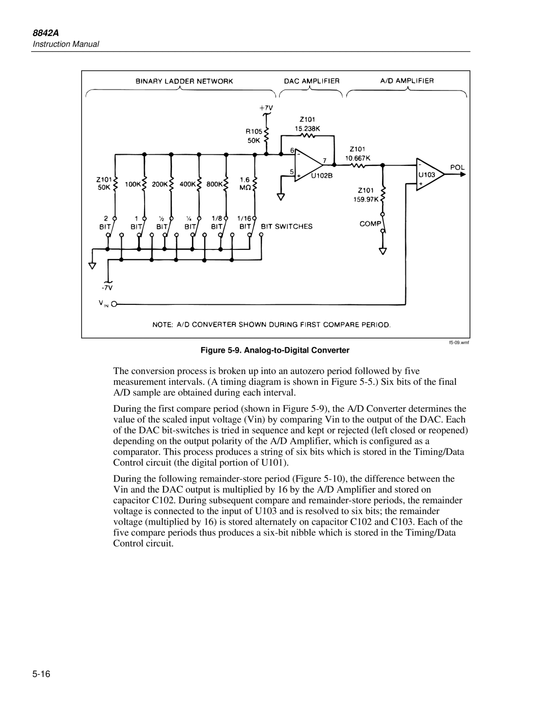
Analog-to-Digital Converter
Precision DAC
Timing/Data Control
Bootstrap Supplies
Display
23. A/D Amplifier
Digital Controller
Keyboard
13. Digital Controller Block Diagram
In-Guard Microcomputer
14. Read/Write Timing Diagrams for Internal Bus
Calibration Correction
Slow Medium Fast Power Line Frequency
Function and Range Control
30. A/D Control and Computation
Guard-Crossing Communication
Troubleshooting Modes
Guard Crossing
Keyboard/Display Control
Power Supply
Bus Interface Circuitry
IEEE-488 Interface Option
Out-Guard Microcomputer
Guard Crossing
Signal Conditioning
IEEE-488 Interface Power Supply
VAC Scaling
MA AC Scaling
Frequency Response Trimming
True RMS AC-to-DC Conversion
Static awareness
Dow Chemical
Maintenance
External Trigger Polarity Selection Option -05 Only
Instrument Type
Minimum Specifications Recommended Model
Frequency Range Minimum Required Accuracy All Ranges
Performance Test
DC Voltage Test
Slow Medium Fast MIN MAX
Step Range Input
Voltage Frequency
AC Voltage Test Option -09 Only
New Offset must be stored for each new range selected
Resistance Test
Fast MIN MAX
DC Current Test
Displayed Reading
Slow Medium MIN MAX
Input Current Frequency
Calibration
AC Current Test Option -09 Only
Step Number Range
Initial Procedure
Basic Calibration Procedure
Calibration Functions
12. A/D Calibration
L O W a B L E Error
Step Displayed Prompt
Step Input
Offset and Gain Calibration
Step
Displayed Prompt VDC VAC1
HIGH-FREQUENCY AC Calibration
Advanced Features and Special Considerations
Storing Variable Inputs
Step Displayed PROMPT1,2
Procedure Function LOW Prompt High Prompt
Calibrating Individual Ranges
Verifying Calibration
Tolerance Check
Erasing Calibration Memory
Tolerance
AC Calibration AT Other Frequencies
Optimizing USE of the 5450A
Calibration
Optimizing Use of the 5450A
Remote Calibration
Front Panel Feature
Corresponding Command
Comments
8842A
Timing Considerations
Example Calibration Program
Remote Erasure
Example A/D Calibration Program
Disassembly Procedure
Case Removal
A Disassembly
F6-062.wmf
F6-063.wmf
F6-064.wmf
True RMS AC PCA Removal Option -09 Only
IEEE-488 Interface PCA Removal Option -05 Only
Main PCA Removal
Maintenance
Front Panel Disassembly
Reassembly Procedure
Reassembly Procedure
Front Panel Disassembly
Removing the Display Window
Internal Fuse Replacement
Troubleshooting
Initial Troubleshooting Procedure
Troubleshooting
16. Overall State Table
T6-162.wmf
17. Circuitry Tested by the Analog Self-Tests
Diagnostic Self-Tests
Self-Test Descriptions
Test Number
Test Point Voltage
Maintenance
8842A
IN-GUARD Microcomputer System
Digital Controller Troubleshooting
In-Guard Microcomputer
Address Latch U219
Display System
Calibration Memory U220
Display Control U212
To-8 Strobe Decoder U213
Analog Control Signals
Device REF. DES
Evaluating Static Signals
21. Analog Control Logic States
DC Scaling Troubleshooting
Evaluating Dynamic Signals
Supply Voltage
PIN or Device
Ohms Current Source Troubleshooting
Track/Hold Troubleshooting
13. Typical Output Waveforms for Track/Hold Circuit TP103
Precision Voltage Reference Troubleshooting
14. Output of A/D Amplifier TP101
66. A/D Converter Troubleshooting
15. Waveforms at U101-24 and U101-25
For fire protection, use exact fuse replacement only
Power Supply Troubleshooting
17. Waveforms at TP102 for Several Inputs on 2V DV Range
Minimum Maximum
Test Point
IEEE-488 Interface Troubleshooting Option
Service Position
Diagnostic Program
Switches Configuration
Troubleshooting
Port BIT
True RMS AC Troubleshooting Option
Major Problems
Defective Ranges
Defective Stage
Input Voltage
Voltage AT TP801
Voltage AT TP802
More Obscure Problems
Internal Cleaning
Guard Crossing Troubleshooting
Cleaning Printed Circuit Assemblies
21. Guard Crossing Test Waveforms
Cleaning After Soldering
8842A
List of Replaceable Parts
8842A
Manual Status Information
HOW to Obtain Parts
Newer Instruments
Service Centers
Assembly Fluke Part no
REF of Option no
Revision Level
F7-011.wmf
F7-012.wmf
F7-013.wmf
F7-014.wmf
A1 Main PCA
CABLE, Display HEADER,1 ROW,.156CTR,6 PIN
8842A
F7-03.wmf
A2 Display PCA
F7-03.wmf
Supply Codes for Manufacturers
Supply2.wmf
Service Centers
Service2.wmf
8842A
Options and Accessories
8842A
Model
Description
Number Option
Accessories
Current Shunt 80J-10
Current Probes Y8100, Y8101, 80i-400
High Voltage Probes 80K-6 and 80K-40
8842A
Option -05 IEEE-488 Interface
805-2
External Controls
Maintenance
Programming Instructions
List of Replaceable Parts
List of Replaceable Parts
805-6
805-7
805-8
Option -09 True RMS AC
809-2
Option -09 True RMS AC
Operating Instructions
809-5
Option -09 True RMS AC PCA
809-7
809-8
Schematic Diagrams
8842A
Schematic Diagrams
F9-012.wmf
Main PCA, A/D Converter
F9-022.wmf
Main PCA, Ohms Current Source
F9-032.wmf
Main PCA, Digital
F9-042.wmf
Main PCA, Power Supply
F9-052.wmf
Display PCA
F9-062.wmf
F9-071.wmf
F9-072.wmf
IEEE-488 Interface PCA, Option
IEEE-488 Interface PCA, Option -08