7 at• J½p
Memory Controller Hub (8240)
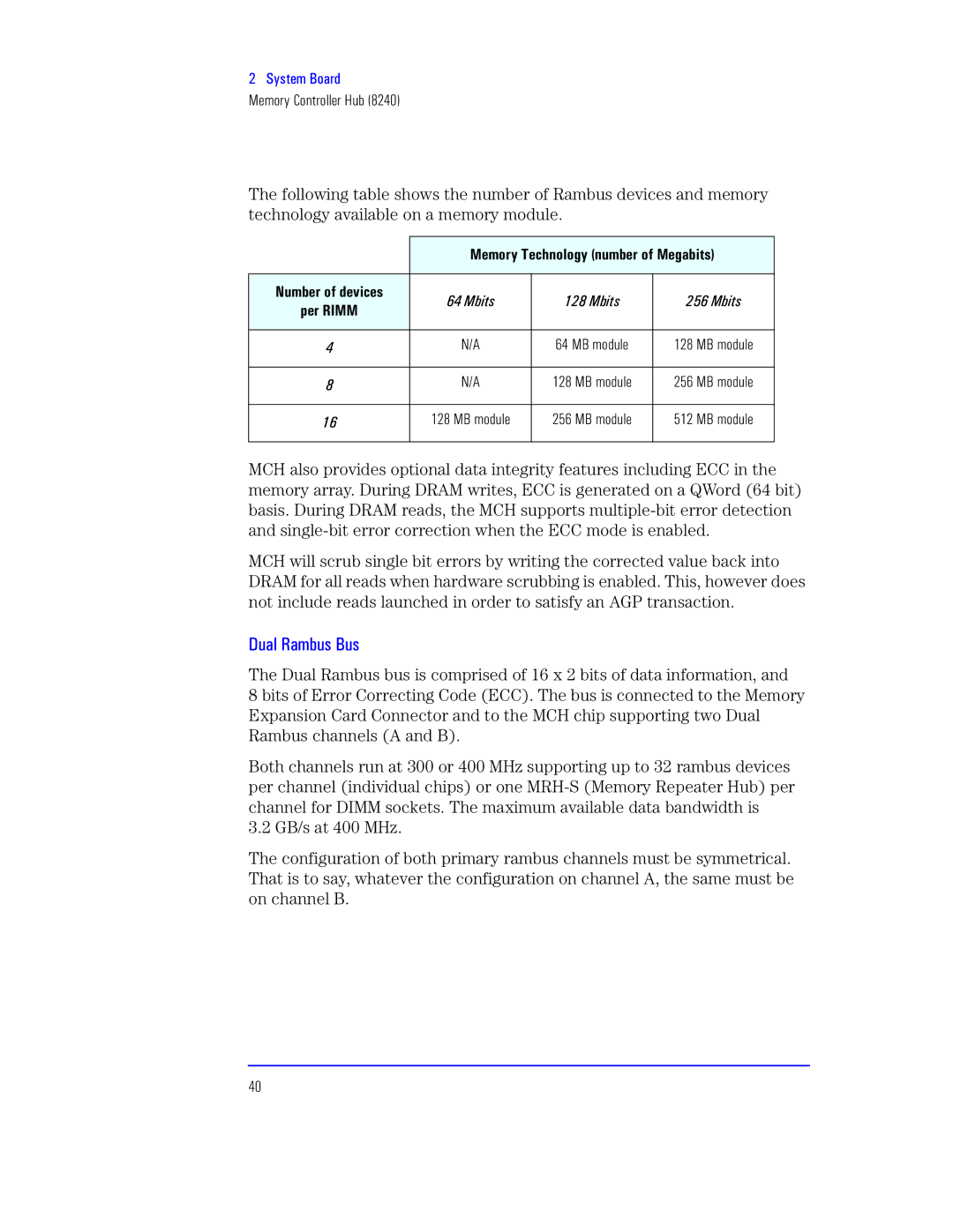
The following table shows the number of Rambus devices and memory technology available on a memory module.
| Vtbtrw®v |
|
| |
|
|
|
|
|
Wqt st | DB d | 8:F d |
| :CD d |
RVV |
| |||
|
|
|
| |
|
|
|
|
|
B | N/A | 64 MB module |
| 128 MB module |
|
|
|
|
|
F | N/A | 128 MB module |
| 256 MB module |
|
|
|
|
|
8D | 128 MB module | 256 MB module |
| 512 MB module |
|
|
|
|
|
MCH also provides optional data integrity features including ECC in the memory array. During DRAM writes, ECC is generated on a QWord (64 bit) basis. During DRAM reads, the MCH supports
MCH will scrub single bit errors by writing the corrected value back into DRAM for all reads when hardware scrubbing is enabled. This, however does not include reads launched in order to satisfy an AGP transaction.
Lp“ ‘p•q
The Dual Rambus bus is comprised of 16 x 2 bits of data information, and
8 bits of Error Correcting Code (ECC). The bus is connected to the Memory Expansion Card Connector and to the MCH chip supporting two Dual Rambus channels (A and B).
Both channels run at 300 or 400 MHz supporting up to 32 rambus devices per channel (individual chips) or one
The configuration of both primary rambus channels must be symmetrical. That is to say, whatever the configuration on channel A, the same must be on channel B.
40
