August
Page
Contents
8XC196LX Supplement Chapter Synchronous Serial I/O Port
Internal Timing
Entering and Exiting Once Mode
Functional Groupings of Signals Default Conditions
Programming the J1850 Controller
Figures
11-3
Tables
Guide to This Manual
Page
Chapter Guide to this Manual
Manual Contents
Related Documents
Related Documents
Architectural Overview
Page
Features of the 8XC196Lx and 8XC196Kx Product Famiies
Microcontroller Features
Chapter Architectural Overview
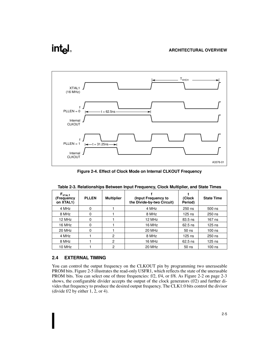
Internal Timing
Block Diagram
Clock Circuitry 87C196LA, LB Only
16 MHz
State Times at Various Frequencies
MHz
12 MHz
Pllen
External Timing
Multiplier State Time
Uprom Programming Values and Locations
Internal Peripherals
CLK1 CLK0
4 J1850 Communications Controller
1 I/O Ports
Synchronous Serial I/O Port
Event Processor Array
Page
Address Space
Page
Address Partitions
Chapter Address Space
Address Map
1BFF
Register File
CA,JT,KT
Address
JR, KR
XC196Lx Peripheral SFRs
Peripheral SPECIAL-FUNCTION Registers
USFR1 LA, LB
Jdly
SSIO1CLK
SSIO0CLK
Rstsrc
Windows
Windowing
Upper Register File CA, JT, JV, KT
Base
Upper Register File CA, JT, JV, KT, LA, LB
0140H
4BH
25H 0120H 49H 0100H 48H 24H 12H
Standard and PTS Interrupts
Page
Interrupt SOURCES, VECTORS, and Priorities
Chapter Standard and PTS Interrupts
Interrupt Source Mnemonic Priority Name
Interrupt Controller PTS Service
Interrupt Registers
Interrupt Sources, Vectors, and Priorities
Bit Mnemonic Interrupt Description
Interrupt Mask Registers
Intmask
Bit Function Number
NMI Extint SSIO1 SSIO0
Interrupt Pending Registers
INTMASK1
LA, LD
Intpend
Interrupt Pending Intpend Register
INTPEND1
Peripheral Transaction Server Registers
NMI
Bit
Ptssel
Interrupt PTS Vector
Bits
Ptssrv
Interrupt Standard Vector
Ports
Page
EPA, Ssio
Chapter Ports
I/O Ports Overview
Microcontroller Ports
8XC196LX Supplement
Ports 1, 2, 5, and 6 Internal Structure 87C196LA, LB Only
Configuring Ports 1, 2, 5, and 6 Bidirectional Ports
Special Bidirectional Port Considerations
For complementary output configurations
Internal Structure for Ports 3 and 4 ADDRESS/DATA BUS
8XC196L X Supplement
Synchronous Serial Port
Page
For receptions
Chapter Synchronous Serial I/O Port
Ssio 0 Clock Register
Bit Function
CHS
Ssio 1 Clock Register
1FB7H
CHS DUP Conint Conpnd Phas Pols
SSIO1CLK
Page
Event Processor Array
Page
Device Capture/Compare Compare-only
Chapter Event Processor Array
EPA Functional Overview
EPA Channels
EPA Block Diagram 87C196LA, LB Only
EPA Block Diagram 83C196LD Only
Epamask
EPA Mask Registers
EPAMASK1
Epapend
EPA Pending Registers
EPAPEND1
Value Interrupt
EPA Interrupt Priority Vector Register
Epaipv
J1850 Communications Controller
Page
J1850 Functional Overview
J1850 Communications Controller
PLL Clkout
J1850 Communications Controller Block Diagram
Control and Status Registers
J1850 Controller Signals and Registers
J1850 Controller Signals
Signal
Control State Machine
J1850 Controller Operation
Cyclic Redundancy Check Generator
Bit Arbitration
Symbol Synchronization and Timing Circuitry
Bus Contention
Error Detection
Digital Filter
Delay Compensation
Symbol Encoding and Decoding
Clock Prescaler
Bit Arbitration Example
Huntzicker Symbol Definition for J1850
Bit Arbitration Example
Message Frames
Normalization Bit
Standard Messaging
Header
CRC Byte
64µS 128µS NB for IFR with CRC NB for IFR without CRC
Name Symbol Bus Level TXmin TXnom TXmax RXmin RXmax Units
Huntzicker Symbol Timing Characteristics
IFR Messaging Type 1 Single Byte, Single Responder
In-frame Response Messaging
Transmitting Messages
Transmitting and Receiving Messages
CPU JTX Jtxbuf
Transmit Byte
Receive Byte
Receiving Messages
CPU Jrxbuf
IFR Messages
Programming the J1850 Command Jcmd Register
Programming the J1850 Controller
MSG30 Operation Purpose
Jcmd
Auto IFR Ignore Abort MSG3 MSG2 MSG1 MSG0
Auto
IFR without CRC Byte
Programming the J1850 Configuration Jcfg Register
NBF IFR3 4XM Txbrk Rxpol PRE1 PRE0
NBF
PRE1 PRE0
Programming the J1850 Delay Compensation Jdly Register
18. J1850 Delay Jdly Register
Jstat
Programming the J1850 Status Jstat Register
Msgrx
Msgtx
Minimum Hardware Considerations
Page
Minimum Hardware Considerations
Identifying the Reset Source
Design Considerations for 8XC196LA, LB, and LD
Special Operating Modes
Page
Chapter Special Operating Modes
Entering and Exiting Once Mode
10-3
Page
Programming Nonvolatile Memory
Page
Signature Word and Programming Voltage Values
Programming the Nonvolatile Memory
Signature Word and Programming Voltage Values
Otprom Address MAP
CCB1
Slave Programming Circuit and Address MAP
C196LA, LB Otprom Address Map
Address Range Description Hex
Description Address Comments
Serial Port Programming Circuit
Serial Port Programming Circuit and Address MAP
Do not address
Serial Port Programming Mode Address Map
Description Address Range
A000-FFFFH
Page
Signal Descriptions
Page
Functional Groupings of Signals
Appendix a Signal Descriptions
Table A-1 C196LA Signals Arranged by Functional Categories
Signal Descriptions
Table A-2 C196LB Signals Arranged by Functional Categories
Figure A-2 C196LB 52-pin Plcc Package
Bus Control & Status
Table A-3 C196LD Signals Arranged by Functional Categories
Input Name Pin
Input/Output Cont’d Name Pin
Default Conditions
Port Alternate During RESET# Upon RESET# Power
Table A-5 C196LA, LB Default Signal Conditions
Signals Functions
Table A-6 C196LD Default Signal Conditions
Page
Glossary
Page
ALU
Glossary
BIT
Byte
EPA
DOUBLE-WORD
ESD
Integer
FET
LSW
ISR
LONG-INTEGER
LSB
MSW
MSB
PIC PIH PLL
PTS
PSW
Ptscb
Ralu
QUAD-WORD
SFR
SAR
SHORT-INTEGER
Uart
WDT
VPW
Word
Index
Page
Clkout
Index
Index-2