8XC196LX SUPPLEMENT
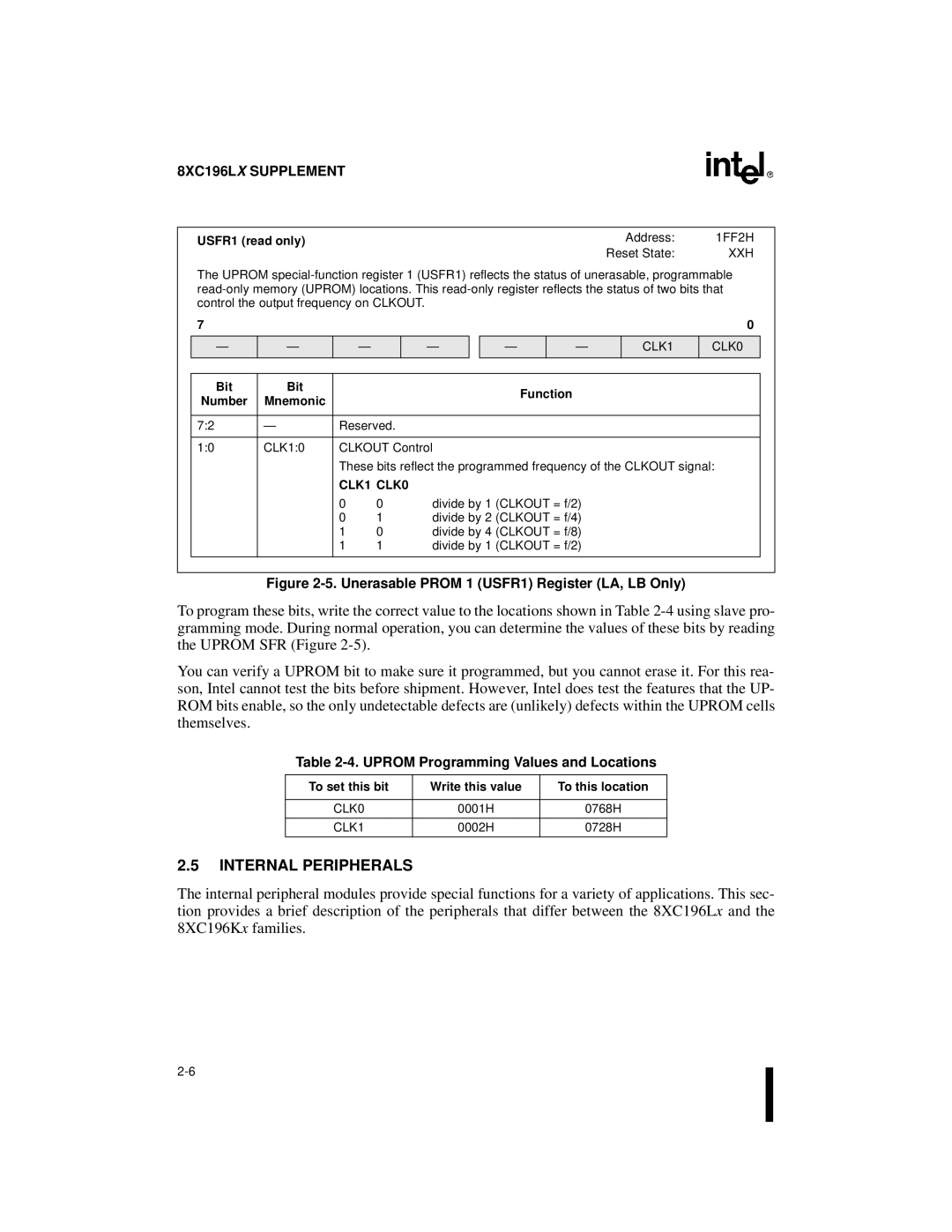
USFR1 (read only) | Address: | 1FF2H |
| Reset State: | XXH |
The UPROM
7 |
|
|
|
|
|
|
|
|
|
| 0 |
— | — |
| — |
| — |
| — |
| — | CLK1 | CLK0 |
|
|
|
|
|
|
|
|
|
|
|
|
Bit | Bit |
|
|
|
|
|
| Function |
|
| |
Number | Mnemonic |
|
|
|
|
|
|
|
| ||
|
|
|
|
|
|
|
|
|
| ||
|
|
|
|
|
|
|
|
|
| ||
7:2 | — | Reserved. |
|
|
|
|
|
|
| ||
|
|
|
|
|
|
|
|
| |||
1:0 | CLK1:0 | CLKOUT Control |
|
|
|
|
|
| |||
|
| These bits reflect the programmed frequency of the CLKOUT signal: | |||||||||
|
| CLK1 CLK0 |
|
|
|
|
|
|
| ||
|
| 0 | 0 |
| divide by 1 (CLKOUT = f/2) |
|
| ||||
|
| 0 | 1 |
| divide by 2 (CLKOUT = f/4) |
|
| ||||
|
| 1 | 0 |
| divide by 4 (CLKOUT = f/8) |
|
| ||||
|
| 1 | 1 |
| divide by 1 (CLKOUT = f/2) |
|
| ||||
|
|
|
|
|
|
|
|
|
|
|
|
Figure 2-5. Unerasable PROM 1 (USFR1) Register (LA, LB Only)
To program these bits, write the correct value to the locations shown in Table
You can verify a UPROM bit to make sure it programmed, but you cannot erase it. For this rea- son, Intel cannot test the bits before shipment. However, Intel does test the features that the UP- ROM bits enable, so the only undetectable defects are (unlikely) defects within the UPROM cells themselves.
Table 2-4. UPROM Programming Values and Locations
To set this bit | Write this value | To this location |
|
|
|
CLK0 | 0001H | 0768H |
|
|
|
CLK1 | 0002H | 0728H |
|
|
|
2.5INTERNAL PERIPHERALS
The internal peripheral modules provide special functions for a variety of applications. This sec- tion provides a brief description of the peripherals that differ between the 8XC196Lx and the 8XC196Kx families.