8XC196LX SUPPLEMENT
8.3.2.1Clock Prescaler
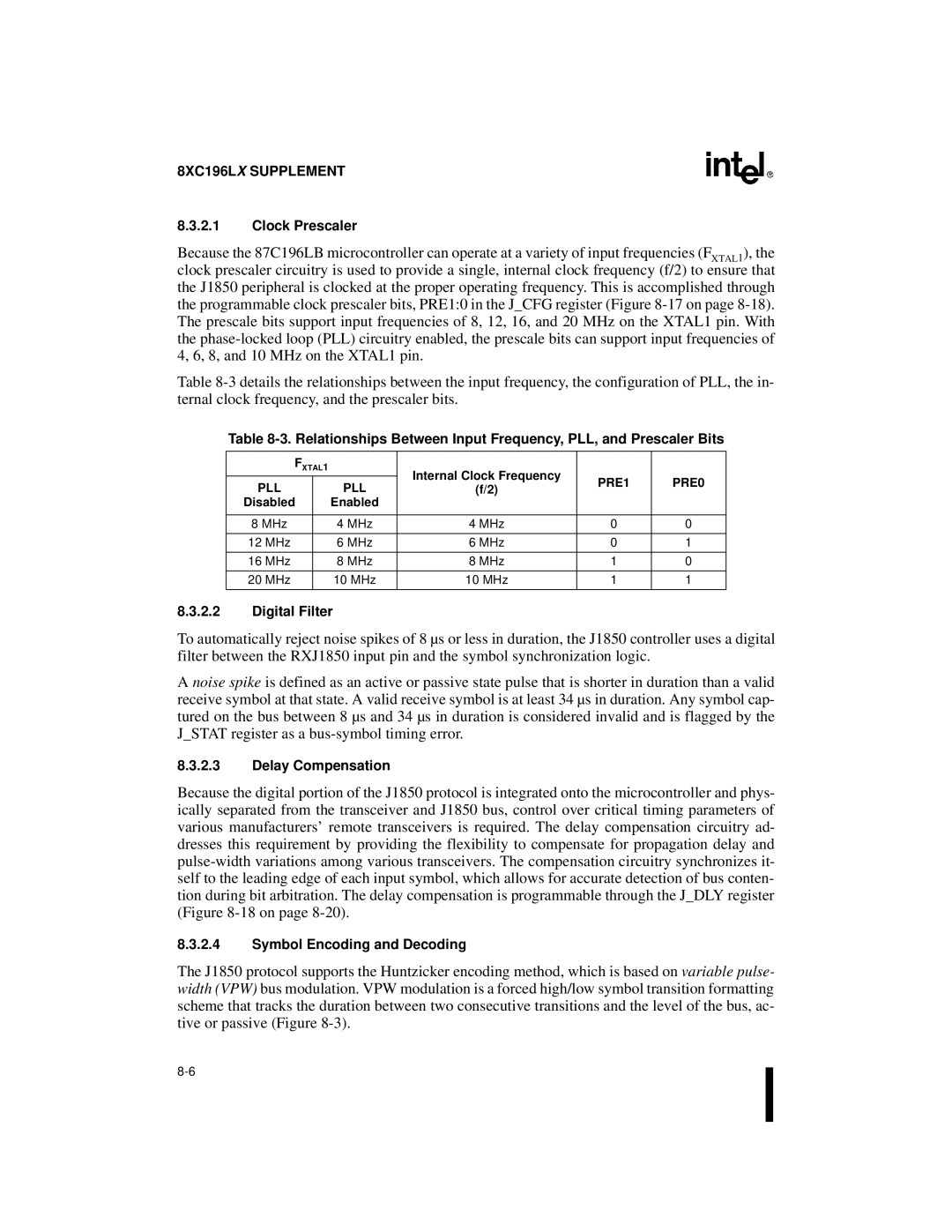
Because the 87C196LB microcontroller can operate at a variety of input frequencies (FXTAL1), the clock prescaler circuitry is used to provide a single, internal clock frequency (f/2) to ensure that the J1850 peripheral is clocked at the proper operating frequency. This is accomplished through the programmable clock prescaler bits, PRE1:0 in the J_CFG register (Figure
Table
Table
FXTAL1 |
| Internal Clock Frequency |
|
| |
PLL |
| PLL | (f/2) | PRE1 | PRE0 |
|
|
| |||
Disabled |
| Enabled |
|
|
|
|
|
|
|
|
|
8 MHz |
| 4 MHz | 4 MHz | 0 | 0 |
|
|
|
|
|
|
12 MHz |
| 6 MHz | 6 MHz | 0 | 1 |
|
|
|
|
|
|
16 MHz |
| 8 MHz | 8 MHz | 1 | 0 |
|
|
|
|
|
|
20 MHz |
| 10 MHz | 10 MHz | 1 | 1 |
|
|
|
|
|
|
8.3.2.2Digital Filter
To automatically reject noise spikes of 8 µs or less in duration, the J1850 controller uses a digital filter between the RXJ1850 input pin and the symbol synchronization logic.
A noise spike is defined as an active or passive state pulse that is shorter in duration than a valid receive symbol at that state. A valid receive symbol is at least 34 µs in duration. Any symbol cap- tured on the bus between 8 µs and 34 µs in duration is considered invalid and is flagged by the J_STAT register as a
8.3.2.3Delay Compensation
Because the digital portion of the J1850 protocol is integrated onto the microcontroller and phys- ically separated from the transceiver and J1850 bus, control over critical timing parameters of various manufacturers’ remote transceivers is required. The delay compensation circuitry ad- dresses this requirement by providing the flexibility to compensate for propagation delay and
8.3.2.4Symbol Encoding and Decoding
The J1850 protocol supports the Huntzicker encoding method, which is based on variable pulse- width (VPW) bus modulation. VPW modulation is a forced high/low symbol transition formatting scheme that tracks the duration between two consecutive transitions and the level of the bus, ac- tive or passive (Figure