Intel 82854 Graphics Memory Controller Hub Gmch
Datasheet
D15343-003
Contents
Intel 82854 Graphics Memory Controller Hub Gmch
10.9
127
Figures
152
Date Revision Description
Revision History
Intel 82854 Graphics Memory Controller Hub Gmch
Processor/Host Bus Support
Overview
Memory System
Video Stream Decoder
System Interrupts
Video Overlay
Display
Internal Graphics Features
Intel 82854 Graphics Memory Controller Hub Gmch
Power Management
Graphic Power Management
Hub Interface to ICH4-M
Package
Intel 854 Chipset system block diagram Native Graphic mode
Terms and Descriptions
Terminology
Term Description
ICH4-M
Reference Documents
Reference Documents
Document Location
Intel 82854 Graphics Memory Controller Hub Gmch
Intel 82854 Gmch
System Architecture
Technology Width
Processor Host Interface
Gmch System Memory Interface
DDR Sdram Memory Capacity
Gmch Integrated DVO Ports
Graphics Features
Display Features
Gmch Analog Display Port
Address Decode Policies
Hub Interface
Bytes MB/s
Gmch Clocking
Intel 82854 Gmch Interface Clocks
Ratio
System Interrupts
Buffer Description
Notation Description
Host Interface Signal Descriptions
Host Interface Signals
HLOCK#
DRDY#
HIT#
HITM#
RS20# Response type
RS20#
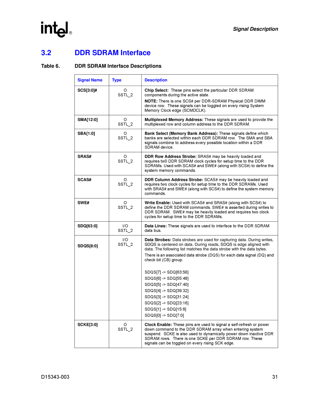
SCAS#
DDR Sdram Interface
DDR Sdram Interface Descriptions
SRAS#
Hub Interface Signals
Hub Interface Signals
Clocks
Drefclk
Display Power Management Signaling This signal is used only
Dpms
DAC Clocking
Digital Video Output B Dvob Port Signal Descriptions
Internal Graphics Display Signals
Digital Video Output B Dvob Port
Digital Video Output C Dvoc Port
Digital Video Output C Dvoc Port Signal Descriptions
Analog CRT Display Signal Descriptions
Dvob and Dvoc Port Common Signal Descriptions
Analog CRT Display
Gpio Signal Descriptions
General Purpose Input/Output Signals
Voltage References, PLL Power
Voltage References, PLL Power
Vcchl
Hlrcomp
Pswing
Hlvref
Device Number Assignment
Conceptual Overview of the Platform Configuration Structure
Gmch Function Bus #0, Device#
Nomenclature for Access Attributes
Nomenclature for Access Attributes
Routing Configuration Accesses
Standard PCI Bus Configuration Mechanism
PCI Bus #0 Configuration Mechanism
Reserved Bits
Primary PCI and Downstream Configuration Mechanism
Default Value upon Reset
Register Definitions
I/O Mapped Registers
Configaddress Configuration Address Register
Reserved
Bit Descriptions
Configuration Data Register
Configdata Configuration Data Register
Name Function Read @ Write @
VGA I/O Mapped Registers
VGA I/O Mapped Register List
Index Data Registers
Register Name Default Value Access
Gmch Configuration Space Device #0, Function#0
End
Attbase
Did Device Identification Register
VID Vendor Identification Register
Bit Descriptions 150
= Serr message is not generated by the Gmch for Device #0
Pcicmd PCI Command Register
PCI Status Register
Subc Sub Class Code Register
RID Register Identification
HDR Header Type Register
BCC Base Class Code Register
Svid Subsystem Vendor Identification Register
Capptr Capabilities Pointer Register
SID Subsystem Identification Register
Capability ID
Capid Capabilities Identification Register Device #0
VGA
Rrbar Access Enable-R/W
GMC Gmch Miscellaneous Control Register Device #0
MDA Present MDAP-R/W
GGC Gmch Graphics Control Register Device #0
Reserved Device #2 Function #1 Enable/Disable
Bit
Fdhc Fixed Dram Hold Control Register Device #0
Dafc Device and Function Control Register Device #0
Bit Description
Attribute Bit Assignment
17 PAM60 Programmable Attribute Map Register Device #0
Bits 7 Bits 6 Bits 5 Bits 4 Description Reserved
PAM Registers
Expansion Area C0000h-DFFFFh
PAM Registers and Associated System Memory Segments
DOS Application Area 00000h-9FFFh
Video Buffer Area A0000h-BFFFFh
System Bios Area F0000h-FFFFFh
Extended System Bios Area E0000h-EFFFFh
Smram System Management RAM Control Register Device #0
Esmramc Extended System Management RAM Control Device #0
Errsts Error Status Register Device #0
Errcmd Error Command Register Device #0
Bit Description Reserved
Smicmd SMI Error Command Register Device #0
SCI on Gmch Thermal Sensor Trip
Scicmd SCI Error Command Register Device #0
Reserved SCI on Multiple-bit ECC Error
SCI on Single-bit ECC Error
Shic Secondary Host Interface Control Register Device #0
Reserved On Die Termination ODT Gating Disable
Reserved FSB Data Bus Power Management Control
C2 state Gmch FSB Interface Power Management Control
HEM Host Error Control, Status, and Observation Device #0
DRB
VID Vendor Identification Register
Pcicmd PCI Command Register
Pcists PCI Status Register
RID Revision Identification Register
Device. Reads and Writes to this location have no effect
DRB Dram Row 03 Boundary Register Device #0
DRA Dram Row Attribute Register Device #0
Examples of usage
DDR Internal Write to Read Command delay tWTR
DDR Write Recovery time tWR
DRT Dram Timing Register Device #0
Refresh Cycle Time tRFC
Encoding CK between RD and WR commands
Back To Back Read-Read commands spacing DDR, different Rows
Encoding CK between RD and RD commands
Activate to Precharge delay tRAS, MIN
Activate to Precharge delay tRAS, MAX
Reserved CAS# Latency tCL
Rcven DLL shutdown disable
PCEn Page Close Enable TC Timer Control PDEn23
CS# Signal Drive Control
Dynamic Memory Interface Power Management
Power State S1/S3 Refresh Control
Ddim DDR Sdram Data Integrity Mode
DRC Dram Controller Mode Register Device #0
011
000
001
010
For Double Data Rate
DTC Dram Throttling Control Register Device #0
Wttc
DDR Sdram Throttle Mode Tmode
2724
High Priority Stream Throttling Enable
Thermal Power Throttle Control fields Enable
Hpllcc
Did Device Identification Register
Pcicmd PCI Command Register
Pcists PCI Status Register
Subc Sub-Class Code Register
ID Subsystem Identification Register
Hpll VCO Change Sequence Initiate Bit
Hpllcc Hpll Clock Control Register Device #0
Rate
Straps Read GFX Core
HPLLCC20
DVO Port CRT Port
Regs
Register Name
Did Device Identification Register Device #2
VID Vendor Identification Register Device #2
Pcicmd PCI Command Register Device #2
RID Revision Identification Register Device #2
Pcists PCI Status Register Device #2
Base Class Code Basec 03=Display controller
MLT Master Latency Timer Register Device #2
CC Class Code Register Device #2
CLS Cache Line Size Register Device #2
Gmadr Graphics Memory Range Address Register Device #2
Bit Description Master Latency Timer Count Value RO
Prefetchable Memory-RO Enable prefetching
HDR Header Type Register Device #2
Memory / IO Space-RO
Mmadr Memory Mapped Range Address Register Device #2
Iobar I/O Base Address Register Device #2
Prefetchable Memory-RO Prevents prefetching
Svid Subsystem Vendor Identification Register Device #2
Romadr Video Bios ROM Base Address Registers Device #2
SID Subsystem Identification Register Device #2
Intrpin Interrupt Pin Register Device #2
Intrline Interrupt Line Register Device #2
Mingnt Minimum Grant Register Device #2
Auxiliary Power Source Hardwired to
Pmcap Power Management Capabilities Register Device #2
Maxlat Maximum Latency Register Device #2
Bits10 Power State
Pmcs Power Management Control/Status Register Device #2
Simplified View of System Address Map
System Memory Address Ranges
Detailed View of System Address Map
DOS Compatibility Area
Compatible Smram Address Range 0A0000h-0BFFFFh
System Memory Segments and Their Attributes
DOS Area 000000h-09FFFFh
Legacy VGA Ranges 0A0000h-0BFFFFh
Monochrome Display Adapter MDA Range 0B0000h 0B7FFFh
Extended System Bios Area 0E0000h-0EFFFFh
System Bios Area 0F0000h-0FFFFFh
Extended System Memory Area
Attributes Comments
1 15 MB-16 MB Window
Pre-allocated System Memory
Pre-allocated System Memory
Dynamic Video Memory Technology Dvmt
Extended Smram Address Range Hseg and Tseg
Hseg
Tseg
PCI Memory Address Range Top of Main System Memory to 4 GB
High Bios Area FFE00000h -FFFFFFFFh
SMM Space Restrictions
System Management Mode SMM Memory Range
SMM Space Definition
5 I/O Address Space
System Memory Shadowing
SMM Space Transaction Handling
PCI I/O Address Mapping
Gmch Decode Rules and Cross-Bridge Address Mapping
Hub Interface Decode Rules
Hub Interface Accesses to Gmch that Cross Device Boundaries
Accesses to Gmch that Cross Device Boundaries
Cycles Initiated Using PCI Protocol
Interface Decode Rules
Relation of DBI Bits to Data Bits
Host Interface Overview
Dynamic Bus Inversion
System Bus Interrupt Delivery
Upstream Interrupt Messages
System Memory Organization and Configuration
Configuration Mechanism for DDR DIMMs
System Memory Interface
Byte Function
DDR Sdram Performance Description
System Memory Register Programming
Data Bytes on DDR Dimm Used for Programming Dram Registers
1 3D/2D Instruction Processing
Integrated Graphics Overview
2.3 3D Primitives and Data Formats Support
Setup Engine
2 3D Engine
Viewport Transform and Perspective Divide
Perspective Correct Texture Support
Backface Culling
Scan Converter
Texture Engine
Anti-Aliasing
Texture Chromakey
Texture Map Filtering
Bump Mapping
Raster Engine
Multiple Texture Composition
Cubic Environment Mapping
Color Dithering
Texture Map Blending
Combining Intrinsic and Specular Color Components
Color Shading Modes
Color Buffer Formats Destination Alpha
Alpha Blending
Depth Buffer
4.1 256-Bit Pattern Fill and BLT Engine
4 2D Engine
Stencil Buffer
Projective Textures
Alpha Stretch BLT
Hardware Cursor Plane Native Graphic Mode only
Dual Display Usage Model Native Graphic Mode only
Planes and Engines
Overlay Plane
Dynamic Bob and Weave
Color Control
Sub-picture Support
Video Functionality
MPEG-2 Decoding
Hardware Motion Compensation
Pipe a Timing Generator Unit
Internal Graphic Display Interface
Arib Support
1.2 H, V timing signals for active and blank timing
HSYNC/VSYNC Field Timing
Parameters
Interlaced Video Field display
Blend Function
Interlace support for Plane a graphics
Arib 960 X 540 support
DVO Control Data Bits
Interlace support for Video Overlay Window
Timing Register Switching
Integrated Ramdac
Analog Display Port Characteristics
DDC Display Data Channel
146 D15343-003
Power and Thermal Management
General Description of Acpi States
General Description of Supported CPU States
Overview
Internal Thermal Sensor
Hysteresis Operation
Usage
External Thermal Sensor Input
Strapping Signals and Configuration
Strapping Configuration
Pin Name Strap Description Configuration Type Buffer Type
GST20
Intel 82854 Gmch Straps for Frequency/CPU Configuration
FSB Freq DDR Freq Gfx Freq Core Vcc
Ballout and Package Information
Voltage Levels and Ball Out for Voltage Groups
VCC/VSS Voltage Groups
Name Voltage Level Ball out
Ballout Table
Row Column Signal Name
156 D15343-003
D15343-003 157
158 D15343-003
D15343-003 159
160 D15343-003
D15343-003 161
162 D15343-003
D15343-003 163
Package Mechanical Information
Intel 82854 Gmch Micro-FCBGA Package Dimensions Top View
Intel 82854 Gmch Micro-FCBGA Package Dimensions Side View
Intel 82854 Gmch Micro-FCBGA Package Dimensions Bottom View