Sundance Technology
ST201 |
| PRELIMINARY draft 2 |
|
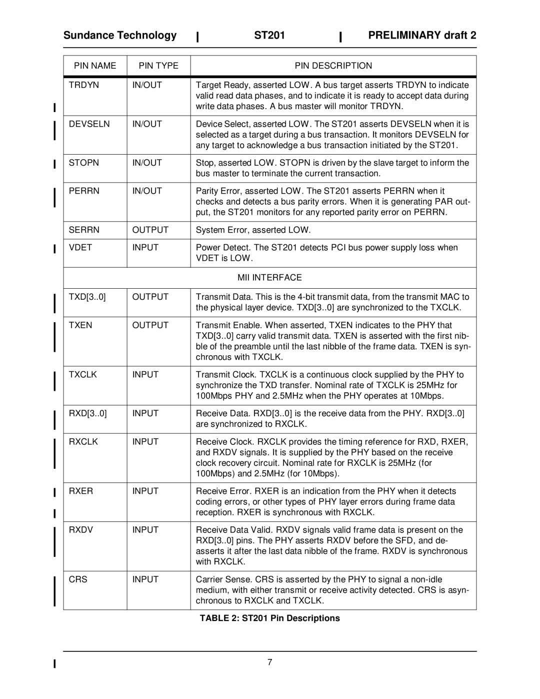
PIN NAME TRDYN
DEVSELN
STOPN
PERRN
SERRN
VDET
PIN TYPE IN/OUT
IN/OUT
IN/OUT
IN/OUT
OUTPUT INPUT
PIN DESCRIPTION
Target Ready, asserted LOW. A bus target asserts TRDYN to indicate valid read data phases, and to indicate it is ready to accept data during write data phases. A bus master will monitor TRDYN.
Device Select, asserted LOW. The ST201 asserts DEVSELN when it is selected as a target during a bus transaction. It monitors DEVSELN for any target to acknowledge a bus transaction initiated by the ST201.
Stop, asserted LOW. STOPN is driven by the slave target to inform the bus master to terminate the current transaction.
Parity Error, asserted LOW. The ST201 asserts PERRN when it checks and detects a bus parity errors. When it is generating PAR out- put, the ST201 monitors for any reported parity error on PERRN.
System Error, asserted LOW.
Power Detect. The ST201 detects PCI bus power supply loss when VDET is LOW.
MII INTERFACE
TXD[3..0] | OUTPUT |
TXEN | OUTPUT |
TXCLK | INPUT |
RXD[3..0] | INPUT |
RXCLK | INPUT |
RXER | INPUT |
RXDV | INPUT |
CRS | INPUT |
|
|
Transmit Data. This is the
Transmit Enable. When asserted, TXEN indicates to the PHY that TXD[3..0] carry valid transmit data. TXEN is asserted with the first nib- ble of the preamble until the last nibble of the frame data. TXEN is syn- chronous with TXCLK.
Transmit Clock. TXCLK is a continuous clock supplied by the PHY to synchronize the TXD transfer. Nominal rate of TXCLK is 25MHz for 100Mbps PHY and 2.5MHz when the PHY operates at 10Mbps.
Receive Data. RXD[3..0] is the receive data from the PHY. RXD[3..0] are synchronized to RXCLK.
Receive Clock. RXCLK provides the timing reference for RXD, RXER, and RXDV signals. It is supplied by the PHY based on the receive clock recovery circuit. Nominal rate for RXCLK is 25MHz (for 100Mbps) and 2.5MHz (for 10Mbps).
Receive Error. RXER is an indication from the PHY when it detects coding errors, or other types of PHY layer errors during frame data reception. RXER is synchronous with RXCLK.
Receive Data Valid. RXDV signals valid frame data is present on the RXD[3..0] pins. The PHY asserts RXDV before the SFD, and de- asserts it after the last data nibble of the frame. RXDV is synchronous with RXCLK.
Carrier Sense. CRS is asserted by the PHY to signal a
TABLE 2: ST201 Pin Descriptions
7