The V.24 Interface
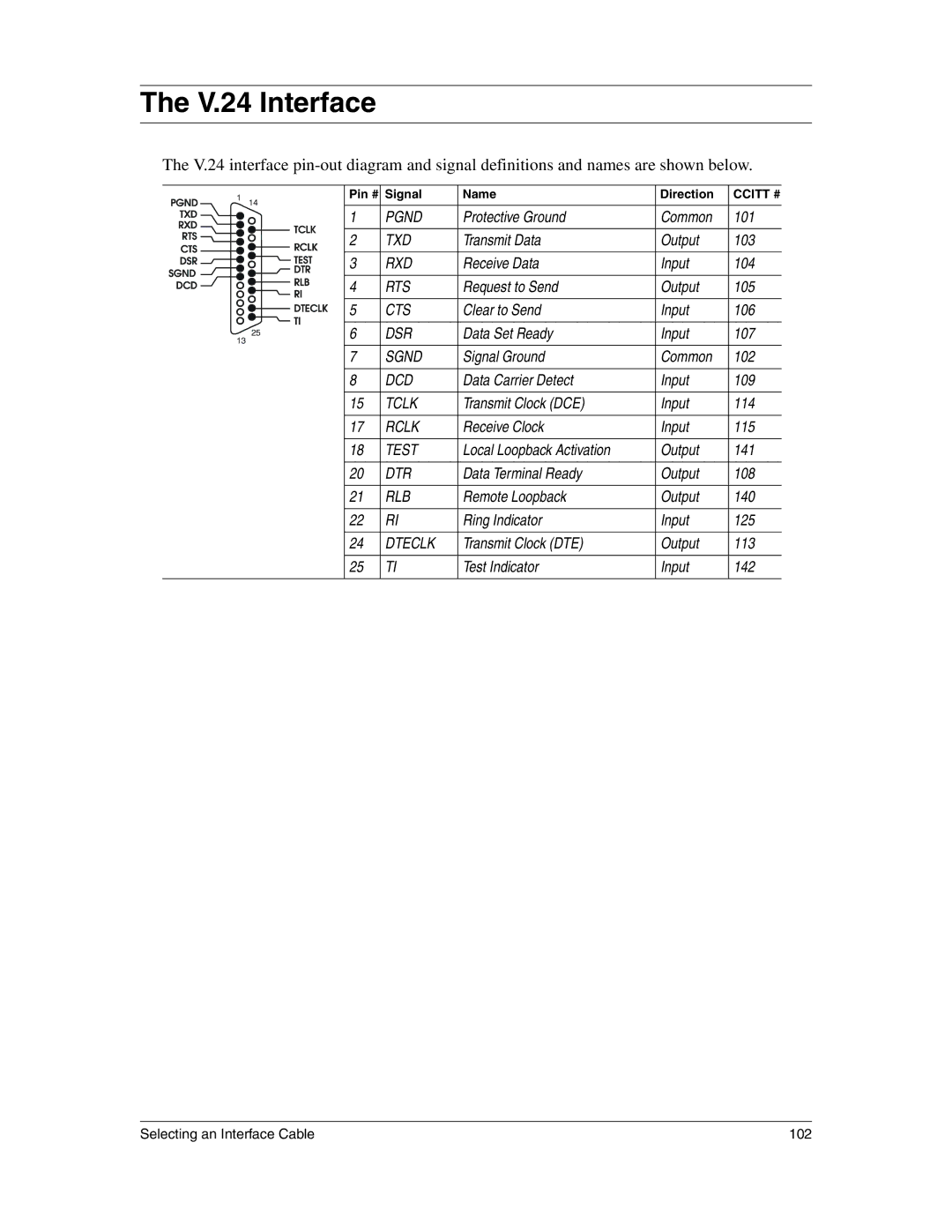
The V.24 interface
|
|
|
|
|
| Pin # | Signal | Name | Direction | CCITT # |
|
|
|
|
|
|
|
|
|
|
|
| 1 | PGND | Protective Ground | Common | 101 | |||||
|
|
|
|
|
|
|
|
|
|
|
| 2 | TXD | Transmit Data | Output | 103 | |||||
|
|
|
|
|
|
|
|
|
|
|
| 3 | RXD | Receive Data | Input | 104 | |||||
|
|
|
|
|
|
|
|
|
|
|
|
|
|
|
|
| 4 | RTS | Request to Send | Output | 105 |
| ||||||||||
| 5 | CTS | Clear to Send | Input | 106 | |||||
|
|
|
|
|
|
|
|
|
|
|
|
| 6 | DSR | Data Set Ready | Input | 107 | ||||
|
|
|
|
|
|
|
|
|
|
|
| 7 | SGND | Signal Ground | Common | 102 | |||||
|
|
|
|
|
|
|
|
|
|
|
| 8 | DCD | Data Carrier Detect | Input | 109 | |||||
|
|
|
|
|
|
|
|
|
|
|
| 15 | TCLK | Transmit Clock (DCE) | Input | 114 | |||||
|
|
|
|
|
|
|
|
|
|
|
| 17 | RCLK | Receive Clock | Input | 115 | |||||
|
|
|
|
|
|
|
|
|
|
|
| 18 | TEST | Local Loopback Activation | Output | 141 | |||||
|
|
|
|
|
|
|
|
|
|
|
| 20 | DTR | Data Terminal Ready | Output | 108 | |||||
|
|
|
|
|
|
|
|
|
|
|
| 21 | RLB | Remote Loopback | Output | 140 | |||||
|
|
|
|
|
|
|
|
|
|
|
| 22 | RI | Ring Indicator | Input | 125 | |||||
|
|
|
|
|
|
|
|
|
|
|
| 24 | DTECLK | Transmit Clock (DTE) | Output | 113 | |||||
|
|
|
|
|
|
|
|
|
|
|
| 25 | TI | Test Indicator | Input | 142 | |||||
|
|
|
|
|
|
|
|
|
|
|
Selecting an Interface Cable | 102 |