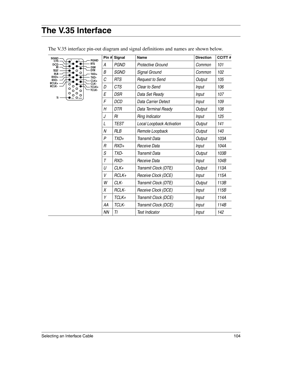
The V.35 Interface
The V.35 interface
|
|
| Pin # | Signal | Name | Direction | CCITT # |
|
|
|
|
|
|
|
|
|
|
| A | PGND | Protective Ground | Common | 101 |
|
|
| B | SGND | Signal Ground | Common | 102 |
|
|
|
|
|
|
|
|
|
|
| C | RTS | Request to Send | Output | 105 |
|
|
|
|
|
|
|
|
|
|
| D | CTS | Clear to Send | Input | 106 |
|
|
|
|
|
|
|
|
|
|
| E | DSR | Data Set Ready | Input | 107 |
|
|
| F | DCD | Data Carrier Detect | Input | 109 |
|
|
|
|
|
|
|
|
|
|
| H | DTR | Data Terminal Ready | Output | 108 |
|
|
|
|
|
|
|
|
|
|
| J | RI | Ring Indicator | Input | 125 |
|
|
|
|
|
|
|
|
|
|
| L | TEST | Local Loopback Activation | Output | 141 |
|
|
|
|
|
|
|
|
|
|
| N | RLB | Remote Loopback | Output | 140 |
|
|
|
|
|
|
|
|
|
|
| P | TXD+ | Transmit Data | Output | 103A |
|
|
|
|
|
|
|
|
|
|
| R | RXD+ | Receive Data | Input | 104A |
|
|
|
|
|
|
|
|
|
|
| S | TXD- | Transmit Data | Output | 103B |
|
|
|
|
|
|
|
|
|
|
| T | RXD- | Receive Data | Input | 104B |
|
|
|
|
|
|
|
|
|
|
| U | CLK+ | Transmit Clock (DTE) | Output | 113A |
|
|
|
|
|
|
|
|
|
|
| V | RCLK+ | Receive Clock (DCE) | Input | 115A |
|
|
|
|
|
|
|
|
|
|
| W | CLK- | Transmit Clock (DTE) | Output | 113B |
|
|
|
|
|
|
|
|
|
|
| X | RCLK- | Receive Clock (DCE) | Input | 115B |
|
|
|
|
|
|
|
|
|
|
| Y | TCLK+ | Transmit Clock (DCE) | Input | 114A |
|
|
|
|
|
|
|
|
|
|
| AA | TCLK- | Transmit Clock (DCE) | Input | 114B |
|
|
|
|
|
|
|
|
|
|
| NN | TI | Test Indicator | Input | 142 |
|
|
|
|
|
|
|
|
Selecting an Interface Cable | 104 |