Epson Stylus Scan
Epson Stylus Scan Revision a
Precautions
Preface
Issued Date
Revision Status
Revision
Description
Epson Stylus Scan Revision a
Contents
Maintenance
Product Description
Local Copy Specifications
Mode Scan Output Print Micro Dot Size Head Media
Mode Res Weave
Local copy
Scan area
Document
Starting scan Edge Position 1st bit Scanning Area
Document
Print area
Print Area
Paper feed direction Printable Area
Raster Graphics mode
Printing
Input data buffer
Control codes
Paper
Printable Area for Envelopes
Envelope Margin
Size Left Margin Right Margin Top Margin Bottom Margin Min
9 Ink
Color Ink Cartridge
Scanner
AAS
Safety, EMC Electrical specifications
Common
Humidity % Temperature C
Environmental conditions
Resistance to electric noise
Reliability
Interfaces
Printer Interface
Parallel
USB Configuration
USB Preventing Data Transfer TIME-OUT of Hosts
Interface Selection
Pin #2 Pin #1
Scanner interfaces
IEEE1284.4 Protocol
Scanner Configuration for USB
USB
Element Description
10. Power-on functions
11. Special settings mode
Control Panel
Buttons
Copy Button
12. Copy button functions
100% B&W Normal Quality Reduce Button Enlarge Number Color
Warm up
13. Settings Menu
LCD
Indicators and LCD Display
14. LCD display and LED indicators
Initialization
Printer Initialization
15. Initialization
Settings Menu
16. Settings Menu
Scanner Initialization
Stylus Scan Errors
PRINTER-SPECIFIC Errors
17. Printer-SPECIFIC errors
Menus
SCANNER-SPECIFIC Errors
Options
Scanning
ADF
Physical Characteristics
Dimensions
Weight
Page
Operating Principles
General
Printer Mechanism Operation
Motor Types and Corresponding Functions
Motor Type Function For details
Printing Mechanism
PF motor
Pump unit
CR guide shaft CR Motor PF roller PG lever
Nozzle selector Board
Sensor
Ink cartridge
Piezo unit Filter
Printing Process
Normal State
Ink course Piezo unit Cavity Ejecting State
Nozzles
Carriage Motor Specifications
CR Motor Control for Each Mode
Phase drive
Carriage Mechanism and Motor
Platen GAP Lever
Motor
Unit Forward
Normal
Motor Control for Each Mode PF Motor Specifications
Paper Feeding Mechanism
Paper Feeding Mechanism Top View
MULTI-FEED Prevention Mechanism
Multiple Paper Loading Prevention Mechanism right side view
Smaller TRAILING-EDGE Margin
Method
Power off sequence
Power on sequence
Carriage Lock Mechanism
Paper eject sequence
Paper PICK-UP Operation
Combination 12.4,28 Eject roller transmission Gear
Pump, Carriage Lock, Head Cleaner Mechanism
Carriage lock Lever Cleaner blade
Ink System
Pump roller Cap unit
Pump Motor Rotation and Function
Gear B Compression Spring Gear C Pump drive Roller
Pump Mode Revolutions Absorption
Pumping modes
Cap Mechanism
Scanner Principles
Carriage Unit
Carriage Operation
20. Carriage Movement
Local and PC Copy Principles
Local copy process
Stylus Scan 2500 Local Copy
Dpi Type Removal
PC Copy Settings
Mode Setting Scan Res. dpi Print Res. dpi Media
PC copy process
Normal PC copy
Electrical Circuit Operating Principles
1 B102 PSB/PSE Board
Application of DC Voltage
Voltage Application Printer Scanner
Power signal
ZD53 Switch
D89 D51 C51,C52 Power drop
Circuit Switch
2 B102 Main Board
1284 I/F
Option
Transceiver
Unit
Epson Stylus Scan Revision a
Troubleshooting
Unit Level Troubleshooting
Printer Condition and Panel Stat us
Printer/Scanner does not operate at power on
Symptoms and Problem s
Flowchart
Error is detected
Failure occurs during printing
EndEnd
Printer does not feed paper correctly
Control panel operation is abnormal
Printer Related Troubleshooting
Printer-Specific errors
Symptom Condition Cause Check Point Solution
Repair of the Printer Mechanis m
Repair of the Printer Mechanism
Epson Stylus Scan Revision a
Epson Stylus Scan Revision a
Scanner Troubleshooting
User-level Scanner-Specific errors
Service Level Troubleshooting Starts Here
Power problems
Scanner does not initialize
Carriage Unit does not operate
10. Carriage unit crashes into frame
11. The lamp does not light up
13. Scsi Interface Error
14. Parallel Interface Error
12. Poor image quality
15. Option unit malfunction
Troubleshooting Motors and Sensors
16. Motor Resistance and Measurement Procedure
Sensor Name Location Signal Level Sensor Status
17. Sensor Check
Disassembly & Assembly
Overview
When transporting the printer after installing
Assembling or adjusting the printer
Make the specified adjustments when you
When assembling, if an ink cartridge is removed
Specification for Screws
Screw Characteristics
Tools
Tool List
Screw Types and Abbreviations
Head Top Side Body Washer Assembled
Service Checks After Repair
Inspection Checklist for the Stylus Scan
Category Component Item to check Is Check Required?
Epson Stylus Scan Revision a
Disassembly Procedures
Removing the Housing
Removing the rear cover
Removing the control panel assembly
Removing the top cover
Remove three CBS 3x6 screws
Removing the side covers
Removing the scanner support frame
Removing the paper eject assembly
Removing the power supply board upper frame
Remove two screws On the left side
Removal of the B102 PSB/PSE Board
Cable protector Remove two Screws
Removing the printer mechanism
Remove three screws Remove two screws Remove one screw
Removal of the Circuit Board Tray
Remove four screws
Removal of the Printer Consumables
Removing the waste ink pads
Spacer Waste ink tank
Removing the cleaning assembly Pump Cap
When reassembling the cleaning assembly, refer to
Assembly, be careful that the parts do not pop out during
Disassembly and assembly
When assembling the printer, be careful not to crush nor
Removing the Cap and Pump Assemblies
Disassembling the Printer Mechanism
Removing the Printhead Unit
Fastener Head
Nozzle Selector has been enclosed into head
Removing the PF Motor Assembly
Compression Spring
Removing the CR Motor Assembly
No.1
Removing the ASF Assembly
Removing the ASF Assembly
Disassembling the ASF Roller Assembly
Hopper Assembly Brake Leveer Torsion Spring
Paper Feed Roller Assembly
Epson standard color
Black
Removing the Right and Left LD Roller Assembly
When installing the LD roller assembly, make sure
Assembly
That the hooks are hung on the paper feed
Removing the Carriage Assembly
12. Removing the Carriage Assembly
Removing the PF Roller Assembly
Front Paper Guide B Eject Paper Roller Assembly
PF Roller Assembly
Removing the PE Paper Detector Assembly
16. Removing the PE Detector Assembly
Disassembly of the Scanner Mechanism
Removing the HP Detector
HP Detector
Removing the scanner
Removing the lamp
Remove two screws
Removing the scanner power supply board
Removing the scanner assembly from the scanner guide shaft
Remove spring here Remove the FFC
Removing the scanner motor
Frame as described in .7.1.3 above
Adjustment
Required Adjustments
List of Service Procedures That Require Adjustment
List of Required Adjustments
Content of Operation Adjustment Procedure
Printer Adjustment
Adjustment Tools Required
Printer hardware adjustments
Parallelism Adjustment
Left Parallelism Adjustment
Fixing Parallelism Adjustment Bushing
Checking Parallelism
Using the Service-Adjustment Program
Installing the program
Software-based Adjustment Procedures
Service Menu Items
Openning the Start-up menu
Head ID Menu
Adjustment Using the Service-Adjustment Program 118
Adjustment Using the Service-Adjustment Program 119
Production Menu
Adjustment Using the Service-Adjustment Program 121
Bi-D Adjustment
Initial Ink Charge Operation
Head Cleaning Operation
CL2 cleaning operation takes 60 seconds to complete
Head Angular Adjustment
Head Voltage ID Input
Following patterns are printed
Sample of Head Angular Adjustment Pattern
Printhead Securing screw
Scanner Adjustment
Ink draining
Special Menu
Maintenance
Cleaning
Lubrication
Printer lubrication points
Scanner lubrication points
Lubrication Point s
Standard Remarks Pag
Maintenance Overview 131
Maintenance Overview 132
Gear 40.8 No.4
GEAR,8
Roller, Exit
Two Pieces
Maintenance Overview 135
Faces out Carriage Assembly Bottom view
Never apply the oil exceeding 0.6cc
Oil pad Lubricated side
No.3 Gear
GEAR,8 No.6 No.7
No.10 No.8
No.9
Type Name Supply Specification Quantity
Scanner Mechanism
Appendix
Connector
Board Connector Summary
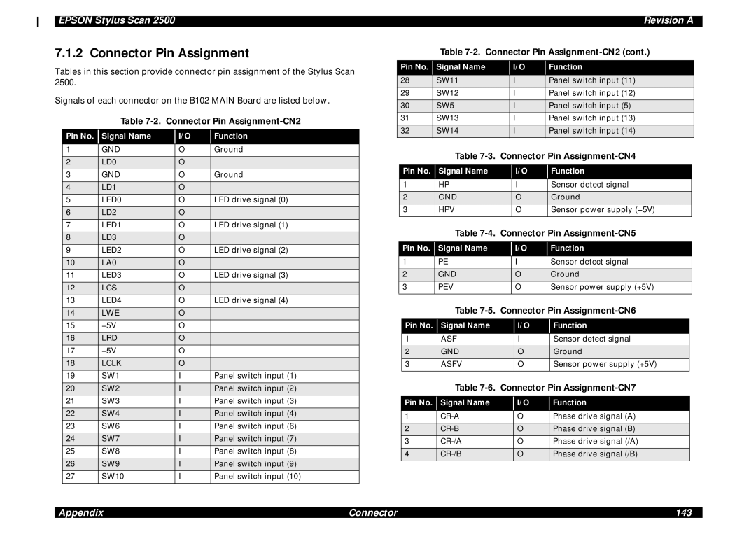
Connector Pin Assignment
Connector Pin Assignment-CN8
Connector Pin Assignment-CN9
Connector Pin Assignment-CN10
10. Connector Pin Assignment-CN11
11. Connector Pin Assignment-CN12
12. Connector Pin Assignment-CN13
13. Connector Pin Assignment-CN1
14. Connector Pin Assignment-CN15
Address Explanation Setting
Settings
Eeprom Address Map
15. Printer Unit Eeprom Address Map
Appendix Eeprom Address Map 147
Appendix Eeprom Address Map 148
16. System Unit Eeprom Map
Appendix Eeprom Address Map 150
Appendix Eeprom Address Map 151
Exploded Diagrams
Appendix Exploded Diagrams 152
Epson Stylus Scan 2500 No.1
Epson Stylus Scan 2500 No.2
Epson Stylus Scan 2500 No.3
Epson Stylus Scan 2500 No.4
Epson Stylus Scan 2500 No.5
Epson Stylus Scan 2500 No.6 Rev.01
Epson Stylus Scan 2500 No.7
Epson Stylus Scan 2500 No.8
Packing Material for Epson Stylus Scan
Parts List
17. Parts List
RefernceNumber Part Name
Appendix Parts List 163
Appendix Parts List 164
Appendix Parts List 165
Appendix Parts List 166
Component Layouts
Appendix Component Layouts 168
Appendix Component Layouts 169
Appendix Component Layouts 170
Appendix Component Layouts 171
Circuit Diagrams
Page
Page
Page