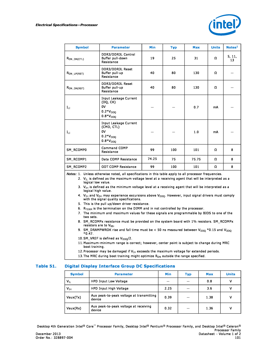
BX80633I74960X, BX80646I34130, BX80646I54430, BX80646I74770K, BX80646I74770 specifications
The Intel CM8063701159502, or BX80637I53470, is a powerful CPU designed for modern computing needs. This processor belongs to Intel's 4th generation of Core i5 processors, commonly known as "Haswell". It showcases Intel's commitment to enhancing performance, increasing energy efficiency, and delivering an enriching user experience.One of the main features of the Intel Core i5-3470 is its quad-core architecture. This allows the processor to handle multiple threads simultaneously, making it adept at multitasking and running demanding applications efficiently. With a base clock speed of 3.2 GHz, it can boost up to 3.6 GHz using Intel’s Turbo Boost technology, providing additional power when needed for intensive tasks like gaming or video editing.
The Intel i5-3470 features Intel's HD Graphics 2500, which offers decent graphics performance for everyday tasks and casual gaming. This integrated graphics solution is capable of delivering high-definition visuals and supports DirectX 11, making it suitable for lightweight gaming experiences without the need for an additional dedicated graphics card.
Another standout characteristic of the BX80637I53470 is its support for Intel Smart Cache, which is an advanced caching technology. It provides a shared cache pool that enhances performance by reducing the time it takes to access frequently used data. This feature, coupled with Intel's instruction set architecture, allows for improved processing agility and efficiency across applications.
The processor is built on a 22nm manufacturing process, which results in reduced power consumption and heat generation compared to its predecessors. It has a thermal design power (TDP) of 77 watts, making it energy efficient while still delivering robust performance. Additionally, the Core i5-3470 supports DDR3 memory, with speeds up to 1600 MHz, enabling quick data retrieval and improved system responsiveness.
Security is another important aspect of the Intel i5-3470, featuring Intel Secure Key and Intel AES New Instructions (AES-NI), which protect sensitive data and enhance encryption performance.
In conclusion, the Intel CM8063701159502, or BX80637I53470, encapsulates modern computing technology with its powerful quad-core performance, integrated graphics, energy efficiency, and robust security features, making it a versatile choice for a wide range of computing tasks. Whether users are engaging in casual gaming, productivity tasks, or multimedia consumption, this processor demonstrates a solid balance of performance and efficiency, providing an excellent computing experience overall.

