MVME172
VME Embedded Controller Programmer’s Reference Guide
Restricted Rights Legend
Preface
Recent Updates
Page
Page
Contents
VMEchip2
Page
Page
MC2 Chip
Xii
IP2 Chip
Chapter Mcecc
Index
Figures
Xvii
Xviii
Introduction
Overview
Board Description and Memory Maps
MVME172 Features Summary
Fuses LAN power SCON, LAN, Fuse LAN power
Feature 200/300-Series
Requirements
Block Diagrams
Functional Description
No-VMEbus-Interface Option
300-Series MVME172 Block Diagram
Block Diagram
500-Series MVME172
Redundant Functions in the VMEchip2 and MC2 Chip
VMEchip2 MC2 Chip Address Bit #
Memory Maps
VMEbus Interface and VMEchip2
Local Bus Memory Map
Normal Address Range
300-Series MVME172 Local Bus Memory Map
Memory Maps
Cache Accessed Width Inhibit
500-Series MVME172 Local Bus Memory Map
Devices Port Software Address Range
Memory Maps
Address Range Devices Accessed Port Size Width
300-Series MVME172 Local I/O Devices Memory Map
$FFFBC000 $FFFBC01F
$FFFBC800 $FFFBC81F
Memory Maps
500-Series MVME172 Local I/O Devices Memory Map
Address Range Device Port Size Width
2KB $FFFBC800 $FFFBC81F
Board Description and Memory Maps
Detailed I/O Memory Maps
Tables 1-7 through 1-17 give the detailed memory maps for
VMEchip2 Memory Map Sheet 1
Offset
This sheet begins on facing
VMEchip2 Memory Map Sheet 2
PRE
Compare Register Counter Overflow
VMEchip2 Memory Map Sheet 3
Offsets Bit Numbers
MC2 Chip Register Map
MC2 Chip Base Address = $FFF42000
Offset D31-D24 D23-D16 D15-D8 D7-D0
IP2 Chip Overall Memory Map
Address Range Selected Device Port Width Size
10. IP2 Chip Memory Map Control and Status Registers
IP2 Chip Base Address = $FFFBC000
DMA
Dlbe
Chani TBL
$51 DMAc INT
Dlbe Ipend Chani TBL Ipto Done
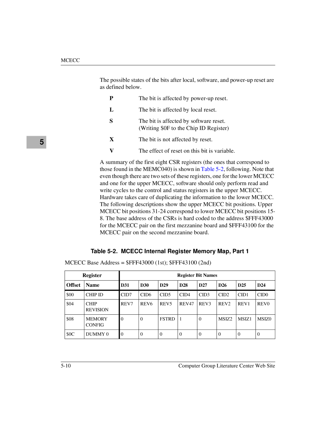
11. Mcecc Internal Register Memory Map
Mcecc Base Address = $FFF43000 1st $FFF43100 2nd
Name D31 D30 D29 D28 D27 D26 D25 D24
12. Z85230 SCC Register Addresses
Z85230 SCC Register Address
13 CA Ethernet LAN Memory Map
14 C710 Scsi Memory Map
BBRAM/TOD Clock Memory Map
15. MK48T58 BBRAM/TOD Clock Memory Map
Address Range Description Size Bytes
16. Bbram Configuration Area Memory Map
Local Scsi ID
17. TOD Clock Memory Map
FT = Frequency Test x = Must be set to
Address Data Bits Function
Ecc1memserial
12 characters are followed by four blanks
3992B03A
VMEbus Memory Map
Interrupt Acknowledge Map
VMEbus Accesses to the Local Bus
Software Support Considerations
Interrupts
VMEbus Short I/O Memory Map
Cache Coherency
Sources of Local Berr
Local Bus Time-out
VMEbus Access Time-out
Local Dram Parity Error
Bus Error Processing
VMEbus Berr
Description of Error Conditions on the MVME172
MPU Parity Error
MPU Off-board Error
MPU TEA Cause Unidentified
MPU Local Bus Time-out
Dmac VMEbus Error
Dmac Parity Error
Dmac Off-board Error
Dmac LTO Error
LAN Parity Error
Dmac TEA Cause Unidentified
LAN Off-Board Error
LAN LTO Error
Scsi Parity Error
Scsi Off-Board Error
Scsi LTO Error
Example of the Proper Use of Bus Timers
MVME172 MC68060 Indivisible Cycles
Illegal Access to IP Modules from External VMEbus Masters
Page
Summary of Major Features
VMEchip2
VMEchip2
Introduction
Functional Blocks
Local Bus to VMEbus Interface
VMEchip2 Block Diagram
VMEchip2
Local Bus to VMEbus Requester
VMEchip2
VMEbus to Local Bus Interface
Functional Blocks
Local Bus to VMEbus DMA Controller
Functional Blocks
No Address Increment DMA Transfers
Dmac VMEbus Requester
Tick and Watchdog Timers
Prescaler
Tick Timers
Watchdog Timer
VMEbus Interrupter
Bus Timer
VMEbus System Controller
Arbiter
Iack Daisy-Chain Driver
Reset Driver
Local Bus Interrupter and Interrupt Handler
Functional Blocks
Lcsr Programming Model
Global Control and Status Registers
Summary of the Lcsr is shown in Table
VMEchip2 Memory Map Lcsr Summary Sheet 1
IO2 IO1
VMEchip2 Memory Map Lcsr Summary Sheet 2
IRQ7 IRQ6 IRQ5
Programming the VMEbus Slave Map Decoders
Lcsr Programming Model
VMEbus Slave Ending Address Register
VMEbus Slave Starting Address Register
VMEbus Slave Address Translation Address Offset Register
VMEbus Slave Address Translation Select Register
Segment Address Translation Size Select Value
$FFF4000C 16 bits
VMEbus Slave Write Post and Snoop Control Register
WP2
SNP2
VMEbus Slave Address Modifier Select Register
DAT
PGM
BLK
A32
USR
SUP
WP1
SNP1
ADDER1
When this bit is high, the first map decoder responds to
Block access cycles
A24 access cycles
Cycles
A32 access cycles
VMEbus supervisory access cycles. When this bit is low
Programming the Local Bus to VMEbus Map Decoders
Bit is low, the first map decoder does not respond to
VMEchip2
Local Bus Slave VMEbus Master Ending Address Register
Local Bus Slave VMEbus Master Starting Address Register
$FFF4001C 16 bits
$FFF40024 16 bits
Local Bus Slave VMEbus Master Attribute Register
D16
Segment defined by map decoder 3. When this bit is
Decoder 3. Because the local bus to VMEbus interface
Segment defined by map decoder 2. When this bit is
Bus map decoder
Decoder 2. Since the local bus to VMEbus interface does
Not support block transfers, the block transfer address
Segment defined by map decoder 1. When this bit is
Decoder 1. Because the local bus to VMEbus interface
VMEbus Slave Gcsr Group Address Register
VMEbus Slave Gcsr Board Address Register
Local Bus to VMEbus Enable Control Register
EN1
EN2
EN3
Local Bus to VMEbus I/O Control Register
I2WP
I2EN
Programming the VMEchip2 DMA Controller
Dmac Command Table Format
Dmac Registers
Entry Function
Prom Decoder, Sram and DMA Control Register
Srams
Tblsc
ROM0
Local Bus to VMEbus Requester Control Register
Lvreql
Lvrwd
Lvfair
DHB
Robn
Dfair
Dtbl
DEN
Dhalt
Tvme
Linc
Vinc
SNP
VME AM
Dmac Local Bus Address Counter
Dmac VMEbus Address Counter
Dmac VMEbus Address Counter
Table Address Counter
VMEbus Interrupter Control Register
Dmac Byte Counter
Irql
Irqs
Irqc
IRQ1S
VMEbus Interrupter Vector Register
MPU Status and DMA Interrupt Count Register
Dmac Status Register
Done
VME
TBL
Programming the Tick and Watchdog Timers
VMEbus Arbiter Time-out Control Register
Vgto
Time on
Lbto
Vato
Prescaler Control Register
Prescaler register = 256 B clock MHz
Tick Timer 1 Compare Register
Tick Timer 1 Counter
Tick timer 1 Compare Register
Tick Timer 2 Compare Register
Tick Timer 2 Counter
Tick timer 2 Counter
Board Control Register
Watchdog Timer Control Register
Tick Timer 2 Control Register
Tick Timer 1 Control Register
Prescaler Counter
Programming the Local Bus Interrupter
Local Bus Interrupter Summary
Interrupt Vector Priority for Simultaneous Interrupts
Dmac
Local Bus Interrupter Status Register bits
LM0
LM1
SIG0
SIG1
SW0
SW1
SW2
SW3
VME1
VME2
VME3
VME4
Local Bus Interrupter Enable Register bits
ELM0
ELM1
ESIG0
ESIG1
ESW0
ESW1
ESW2
ESW3
EIRQ1
EIRQ2
EIRQ3
EIRQ4
Software Interrupt Set Register bits
Interrupt Clear Register bits
Interrupt Level Register 1 bits
Sysf Level WPE Level
Interrupt Level Register 2 bits
SIG3 Level SIG2 Level
Interrupt Level Register 3 bits
SW5 Level SW4 Level
Interrupt Level Register 4 bits
VIRQ6 VIRQ5 Level
Vector Base Register
VBR
Control Register
Connects to pin 16 of the Remote Status and Control
Connects to pin 17 of the Remote Status and Control
Connects to pin 18 of the Remote Status and Control
Miscellaneous Control Register
Enint
100 Computer Group Literature Center Web Site
Gcsr Programming Model
102 Computer Group Literature Center Web Site
Programming the Gcsr
Gcsr Programming Model
Shows a summary of the Gcsr
VMEchip2 Memory Map Gcsr Summary
Local Bus
VMEchip2 Revision Register
VMEchip2 ID Register
VMEchip2 LM/SIG Register
LM2
LM3
VMEchip2 Board Status/Control Register
ISF
RST
General Purpose Register
Local Bus $FFF40110/VMEbus $XXY8 16 bits
Local Bus $FFF40118/VMEbus $XXYC 16 bits
MC2 Chip
MC2 Chip Initialization
Flash and Prom Interface
Bbram Interface
82596CA LAN Interface
MPU Port and MPU Channel Attention
Lanc Bus Error
MC68060-Bus Master Support for 82596CA
53C710 Scsi Controller Interface
Sram Memory Controller
NON-ECC Dram Memory Controller
Lanc Interrupt
Z85230 SCC Interface
Dram Performance
Clock Budget Operating Conditions
Tick Timers
Address Range SCC Device Number
Watchdog Timer
Local Bus Timer
Memory Map of the MC2 Chip Registers
Memory Map of the MC2 Chip Registers
Programming Model
MC2 Chip ID Register
MC2 Chip Revision Register
General Control Register
Interrupt Vector Base Register
SCCIT10 Number of Z85230s
Interrupt Vector Base Register Encoding Priority
Interrupt Source IV3-IV0 Daisy Chain Priority
Programming the Tick Timers
Tick Timer 1 and 2 Compare and Counter Registers
Tick Timer 1 Compare Register
Tick Timer 1 Counter
Tick Timer 2 Compare Register
Tick Timer 2 Counter
LSB Prescaler Count Register
Prescaler Clock Adjust Register
Tick Timer 1 and 2 Control Registers
Tick Timer 2 Control Register
Tick Timer 1 Control Register
OVF3-OVF0
Tick Timer Interrupt Control Registers
Tick Timer 4 Interrupt Control Register
Tick Timer 3 Interrupt Control Register
Tick Timer 2 Interrupt Control Register
Tick Timer 1 Interrupt Control Register
Dram Parity Error Interrupt Control Register
IL2-IL0
Iclr
IEN
SCC Interrupt Control Register
Tick Timer 3 and 4 Control Registers
Tick Timer 4 Control Register
Tick Timer 3 Control Register
Dram and Sram Memory Controller Registers
Dram Space Base Address Register
Sram Space Base Address Register
Dram Space Size Register
Dram Size Control Bit Encoding
DRAM/SRAM Options Register
DZ2 DZ0 Memory Size
Sram Size Control Bit Encoding
F0 set to a 0 indicates that one 28F016SA 2M x 8 Flash
Memory device is used. F0 set to a 1 indicates that four
28F020 256K x 8 Flash memory devices are used
Sram Space Size Register
SZ1 SZ0 Memory Size
Lanc Error Status Register
LTO, EXT, Prty
82596CA Lanc Interrupt Control Register
Plty
Lanc Bus Error Interrupt Control Register
Scsi Error Status Register
General Purpose Inputs Register
V11
MVME172 Version Register
Scsi Interrupt Control Register
Tick Timer 3 and 4 Compare and Counter Registers
Tick Timer 3 Compare Register
Tick Timer 3 Counter
Tick Timer 4 Compare Register
Tick Timer 4 Counter
Bus Clock Register
Prom Access Time Control Register
ET2 Prom Access = N
At 25 MHz where N = At 33 MHz where N =
Flash Access Time Control Register
FT2 Flash Access = N
Abort Switch Interrupt Control Register
Reset Switch Control Register
Watchdog Timer Control Register
Access and Watchdog Time Base Select Register
Wdto These bits define the watchdog time-out period
Bit Time-out Encoding
Dram Control Register
MPU Status Register
PAREN-PARINT
Clock tick
Alternate
Programming Model
Bit Prescaler Count Register
IP2 Chip
General Description
Local Bus to IndustryPack DMA Controllers
IP2 Chip
Clocking Environments and Performance
IP2 Chip Clock Cycles
Error Reporting
Following paragraphs describe the IP2 chip error reporting
Error Reporting as a Local Bus Slave
Error Reporting as a Local Bus Master
IndustryPack Error Reporting
Overall Memory Map
This bit is readable and writable
This status bit is cleared by writing a one to it
IP2 Chip Memory Map Control and Status Registers
Register Register Name Register Bit Names Offset
DMA Rotat
Dint Dien Diclr
Chani TBL
$5B DMAc LB
Dmac for
Chip ID Register
Chip Revision Register
Vector Base Register
IPa, IPb, IPc, IPd Memory Base Address Registers
IV2-0 Interrupt Source
IPa or Double Size IPab Memory Base Address Registers
IPb Memory Base Address Registers
IPa, IPb, IPc, IPd Memory Size Registers
IPc or Double Size IPcd Memory Base Address Registers
Not used on 200/300-Series MVME172
IPd Memory Base Address Registers
BIT NAME$0C
Corresponding INT status bit. In level-sensitive mode
When IEN is set, the interrupt is enabled. When IEN is
Cleared, the interrupt is disabled
When this bit is high, an interrupt is being generated for
IPa, IPb, IPc, and IPd General Control Registers
MEN
BTD
Memory Space Data Width
AERR
BERR
CERR
DERR
Setting IP32 to a one enables the IndustryPack bus to
Setting it to a zero will enable 8 MHz operation. In this
IP Clock Register
IP32
Where each Dmac has equal access to the MC68060
DMA Arbitration Control Register
Local bus. If Rotat is set to a one, the priority is fixed
IP Reset Register
RES
Programming the DMA Controllers
Control Word Byte Count
DMA Enable Function
DMA Control and Status Register Set Definition
DMA Status Register
Ipto
Ipend
DIL2-DIL0
Dien
Dint
DEN
DMA Control Register
Adma
Toip
Ento
Dmaei
DMA Local Bus Address Counter
DMA IndustryPack Address Counter
DMA Byte Counter
DMA Table Address Counter
Programming the Programmable Clock
Programmable Clock Interrupt Control Register
IL2-0
IRE
Programmable Clock General Control Register
PS2-0
CLR
Programmable Clock Timer Register
PLS
Local Bus to IndustryPack Addressing
Bit Memory Space
Comments
Local Bus to IndustryPack Addressing
$00FFFFFB $7FFFFD
IPa I/O Space
IPA6-0 Comments
IPab I/O Space
IPa ID Space
IPA5-0 Comments
Memory Space Accesses
IP to Local Bus Data Routing
This section shows data routing from an IP to the local bus
IP to Local Bus Data Routing
ID Space Accesses
Space Lbsize LBA IPA
Features
Mcecc
Performance
Mcecc Specifications
Descriptions Specifications
ECC
Cycle Types
Error Reporting
Single Bit Error Cycle Type = Burst Read or Non-Burst Read
Double Bit Error Cycle Type = Burst Read or Non-Burst Read
Single Bit Error Cycle Type = Non-Burst Write
Double Bit Error Cycle Type = Non-Burst Write
Triple or Greater Bit Error Cycle Type = Non-Burst Write
Single Bit Error Cycle Type = Scrub
Error Logging
Double Bit Error Cycle Type = Scrub
Triple or Greater Bit Error Cycle Type = Scrub
Scrub
Chip Defaults
Refresh
Arbitration
Programming Model
Mcecc Internal Register Memory Map, Part
Mcecc Base Address = $FFF43000 1st $FFF43100 2nd
Register
Offset Name
Base BAD31 BAD30 BAD29 BAD28 BAD27 BAD26 BAD25 BAD24 Address
Register Bit Names
D31 D30 D29 D28 D27 D26 D25 D24
Scrub SAC7 SAC6 SAC5 SAC4 Addr Cntr
1st $FFF43000/2nd $FFF43100 8-bits
Memory Configuration Register
MSIZ2-MSIZ0
Dummy Register
RB3 Read Bit 3 is a read only bit that is always
RB4 Read Bit 4 is a read only bit that is always
Base Address Register
Difference from MEMC040 none
Bit assignments for the Base Address Register are
Bit assignments for the Dram Control Register are
RWB3 Read/Write Bit 3 is a general purpose read/write bit
RWB5 Read/Write Bit 5 is a general purpose read/write bit
Bclk Frequency Register
Data Control Register
Mcecc
Scrub Control Register
Scrub Period Register Bits
This register contains bits 7-0 of the Scrub Period Register
Chip Prescaler Counter
Scrub Time On/Time Off Register
STOFF2-STOFF0
STON2-STON0
Scrubber Time Off
Scrubber Time On
Scrub Prescaler Counter Bits
Scrub Timer Counter Bits
Scrub Address Counter Bits
1st $FFF4304C/2nd $FFF4314C 8-bits
Error Logger Register
Error Address Bits
1st $FFF43064/2nd $FFF43164 8-bits
Error Syndrome Register
Defaults Register
RSIZ2-RSIZ0
SELI1, SELI0
Dram Array Size
Register Base Address
RESST2-RESST0
Nocache
Initialization
Mcecc
Bank in Error Bit in Error Syndrome Code
Syndrome Decode
Bank C
Bank a
Mcecc
Motorola Computer Group Documents
Document Title Motorola Publication Number
Literature Updates
Manufacturers’ Documents
Table A-2. Manufacturers’ Documents
Table A-2. Manufacturers’ Documents
Related Documentation
BUsing Interrupts on the MVME172
VMEchip2 Tick Timer 1 Periodic Interrupt Example
Step Register and Address Action and Reference
Refer to the Vector Base Register
Using Interrupts on the MVME172
Page
Index
IN-2
DMA
Gcsr
Lanc
IN-6
MPU
SCC
Scsi Mcecc
IN-10
IN-11
Index
MVME172 Programmer’s Reference Guide
MVME172