Hardware Reference
All interface signals are routed to the logic module. The CAN controllers are supported by an AHB interface instantiated into the logic module code example supplied with the
The transmit and receive data signals, CANx_TXD and CANx_RXD, at the EXPIM connectors are not used for the normal operation of the interfaces. They are provided to allow you to implement your own CAN controller logic in the logic module FPGA.
The surface mount links, LK1 and LK2, are provided so that the transmit data signals to the TJA1050 transceivers can be driven either from the CAN controllers or directly from the logic module FPGA.
Table
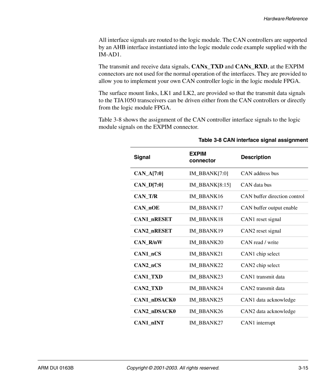
Table 3-8 CAN interface signal assignment
Signal | EXPIM | Description | |
connector | |||
|
| ||
|
|
| |
CAN_A[7:0] | IM_BBANK[7:0] | CAN address bus | |
|
|
| |
CAN_D[7:0] | IM_BBANK[8:15] | CAN data bus | |
|
|
| |
CAN_T/R | IM_BBANK16 | CAN buffer direction control | |
|
|
| |
CAN_nOE | IM_BBANK17 | CAN buffer output enable | |
|
|
| |
CAN1_nRESET | IM_BBANK18 | CAN1 reset signal | |
|
|
| |
CAN2_nRESET | IM_BBANK19 | CAN2 reset signal | |
|
|
| |
CAN_R/nW | IM_BBANK20 | CAN read / write | |
|
|
| |
CAN1_nCS | IM_BBANK21 | CAN1 chip select | |
|
|
| |
CAN2_nCS | IM_BBANK22 | CAN2 chip select | |
|
|
| |
CAN1_TXD | IM_BBANK23 | CAN1 transmit data | |
|
|
| |
CAN2_TXD | IM_BBANK24 | CAN2 transmit data | |
|
|
| |
CAN1_nDSACK0 | IM_BBANK25 | CAN1 data acknowledge | |
|
|
| |
CAN2_nDSACK0 | IM_BBANK26 | CAN2 data acknowledge | |
|
|
| |
CAN1_nINT | IM_BBANK27 | CAN1 interrupt |
ARM DUI 0163B | Copyright © |