Reference Design Example
0xF0000000
0xE0000000
0xD0000000
0xC0000000
Logic module 3
Logic module 2
Logic module 1
Logic module 0
Core module alias memory
PCI
Core module/ motherboard memory
and peripherals
AHB
peripherals
APB peripherals
0xCFFFFFFF
0xC1000000
0xC0000000
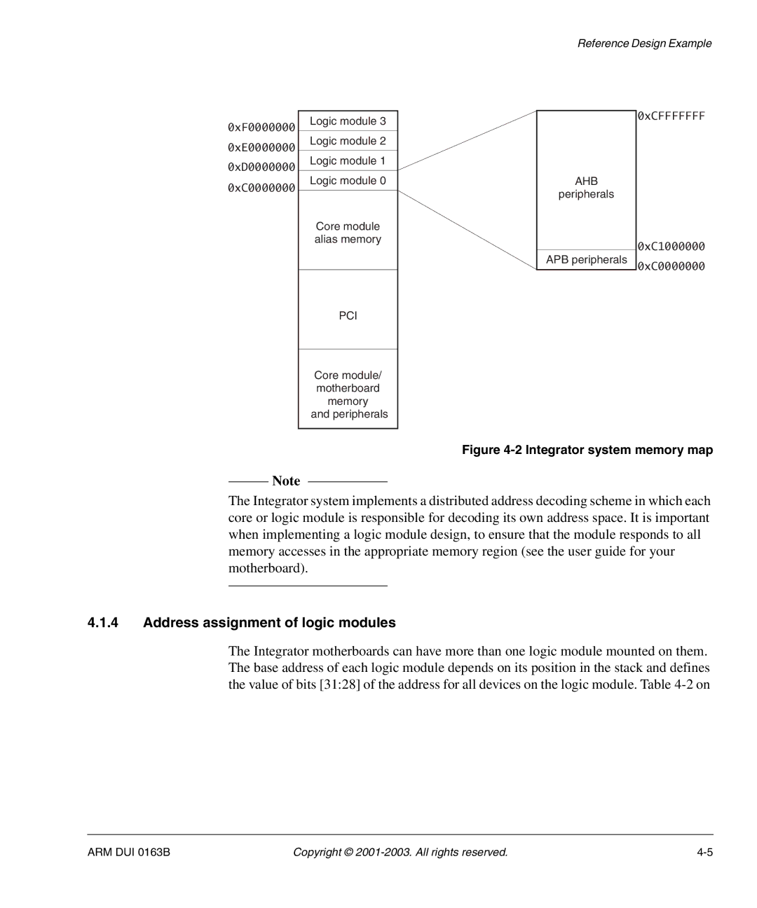
Figure 4-2 Integrator system memory map
Note
The Integrator system implements a distributed address decoding scheme in which each core or logic module is responsible for decoding its own address space. It is important when implementing a logic module design, to ensure that the module responds to all memory accesses in the appropriate memory region (see the user guide for your motherboard).
4.1.4Address assignment of logic modules
The Integrator motherboards can have more than one logic module mounted on them. The base address of each logic module depends on its position in the stack and defines the value of bits [31:28] of the address for all devices on the logic module. Table
ARM DUI 0163B | Copyright © |