Reference Design Example
4.4SPI chip select register
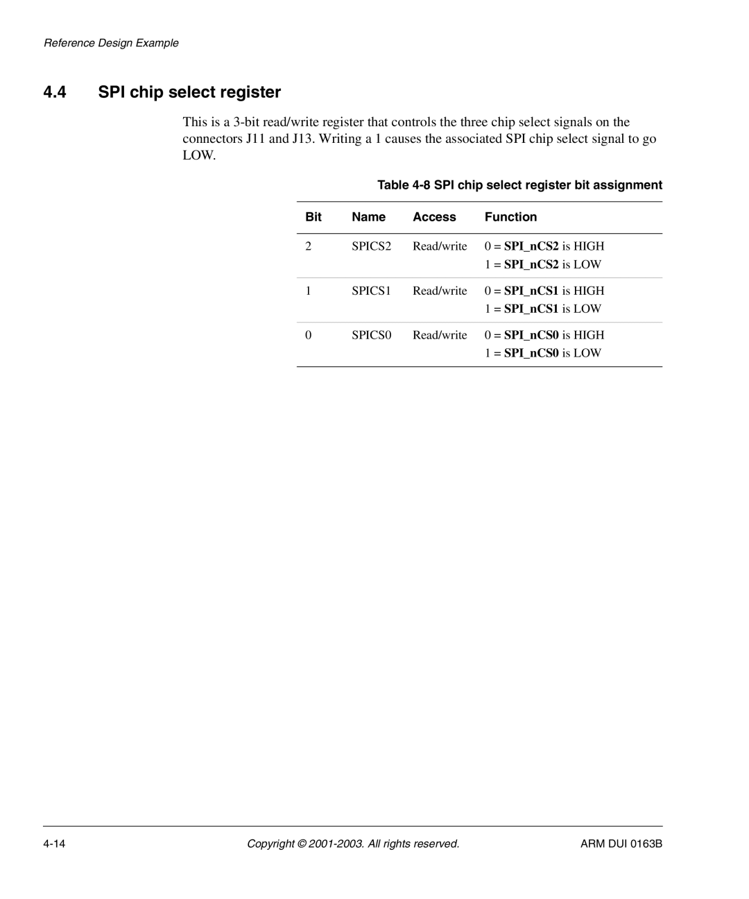
This is a
Table
Bit | Name | Access | Function | |
|
|
|
|
|
2 | SPICS2 | Read/write | 0 | = SPI_nCS2 is HIGH |
|
|
| 1 | = SPI_nCS2 is LOW |
|
|
|
|
|
1 | SPICS1 | Read/write | 0 | = SPI_nCS1 is HIGH |
|
|
| 1 | = SPI_nCS1 is LOW |
|
|
|
|
|
0 | SPICS0 | Read/write | 0 | = SPI_nCS0 is HIGH |
|
|
| 1 | = SPI_nCS0 is LOW |
|
|
|
|
|
Copyright © | ARM DUI 0163B |
