Reference Design Example
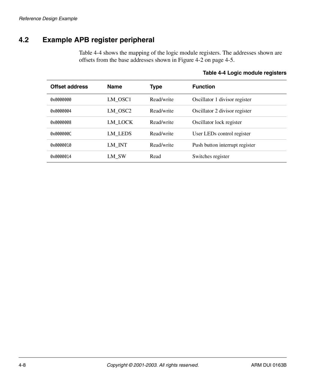
4.2Example APB register peripheral
Table
|
|
| Table |
|
|
|
|
Offset address | Name | Type | Function |
|
|
|
|
0x0000000 | LM_OSC1 | Read/write | Oscillator 1 divisor register |
|
|
|
|
0x0000004 | LM_OSC2 | Read/write | Oscillator 2 divisor register |
|
|
|
|
0x0000008 | LM_LOCK | Read/write | Oscillator lock register |
|
|
|
|
0x000000C | LM_LEDS | Read/write | User LEDs control register |
|
|
|
|
0x0000010 | LM_INT | Read/write | Push button interrupt register |
|
|
|
|
0x0000014 | LM_SW | Read | Switches register |
|
|
|
|
Copyright © | ARM DUI 0163B |
