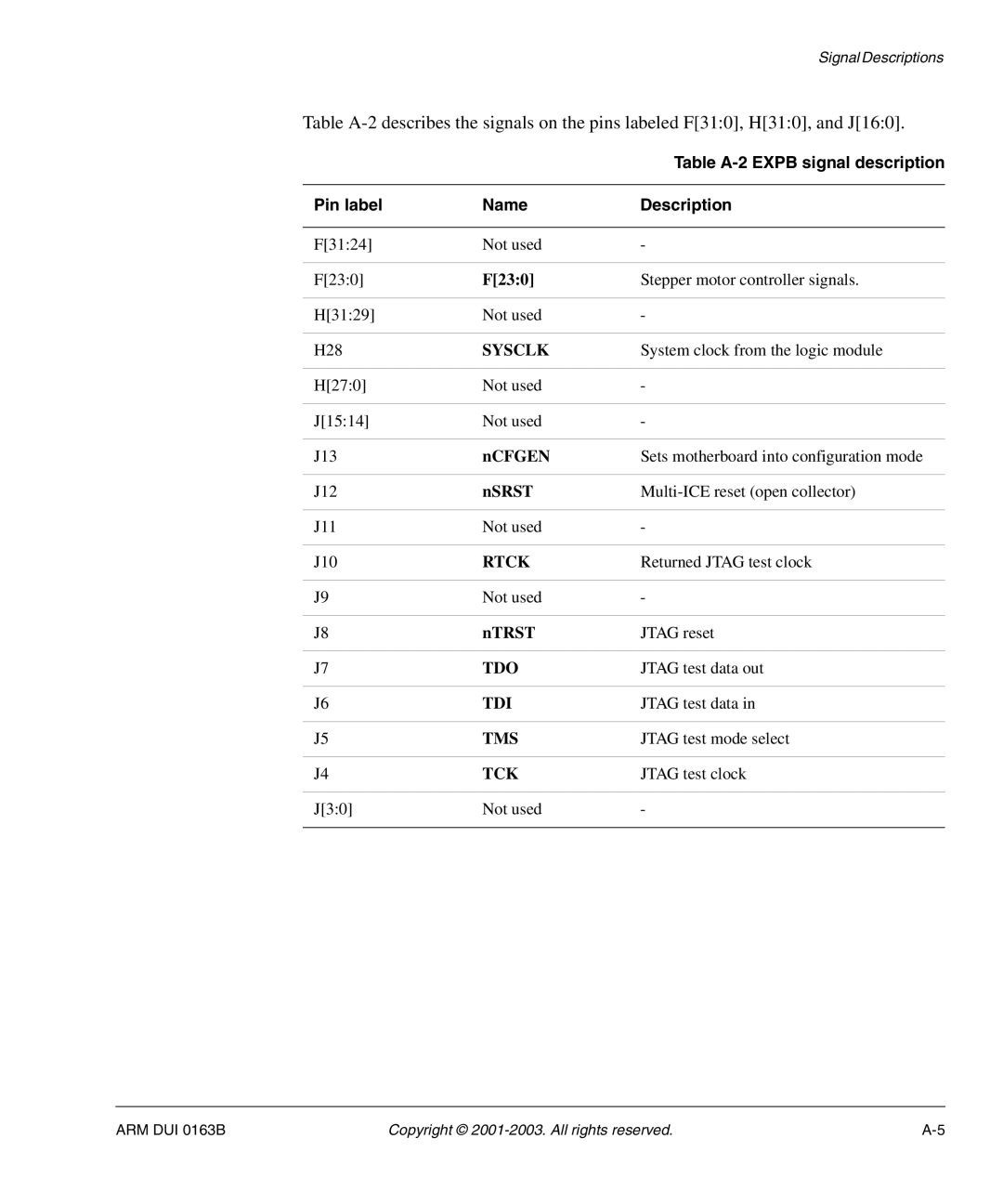
Signal Descriptions
Table
|
| Table |
|
|
|
Pin label | Name | Description |
|
|
|
F[31:24] | Not used | - |
|
|
|
F[23:0] | F[23:0] | Stepper motor controller signals. |
|
|
|
H[31:29] | Not used | - |
|
|
|
H28 | SYSCLK | System clock from the logic module |
|
|
|
H[27:0] | Not used | - |
|
|
|
J[15:14] | Not used | - |
|
|
|
J13 | nCFGEN | Sets motherboard into configuration mode |
|
|
|
J12 | nSRST | |
|
|
|
J11 | Not used | - |
|
|
|
J10 | RTCK | Returned JTAG test clock |
|
|
|
J9 | Not used | - |
|
|
|
J8 | nTRST | JTAG reset |
|
|
|
J7 | TDO | JTAG test data out |
|
|
|
J6 | TDI | JTAG test data in |
|
|
|
J5 | TMS | JTAG test mode select |
|
|
|
J4 | TCK | JTAG test clock |
|
|
|
J[3:0] | Not used | - |
|
|
|
ARM DUI 0163B | Copyright © |