Reference Design Example
4.8GPIO
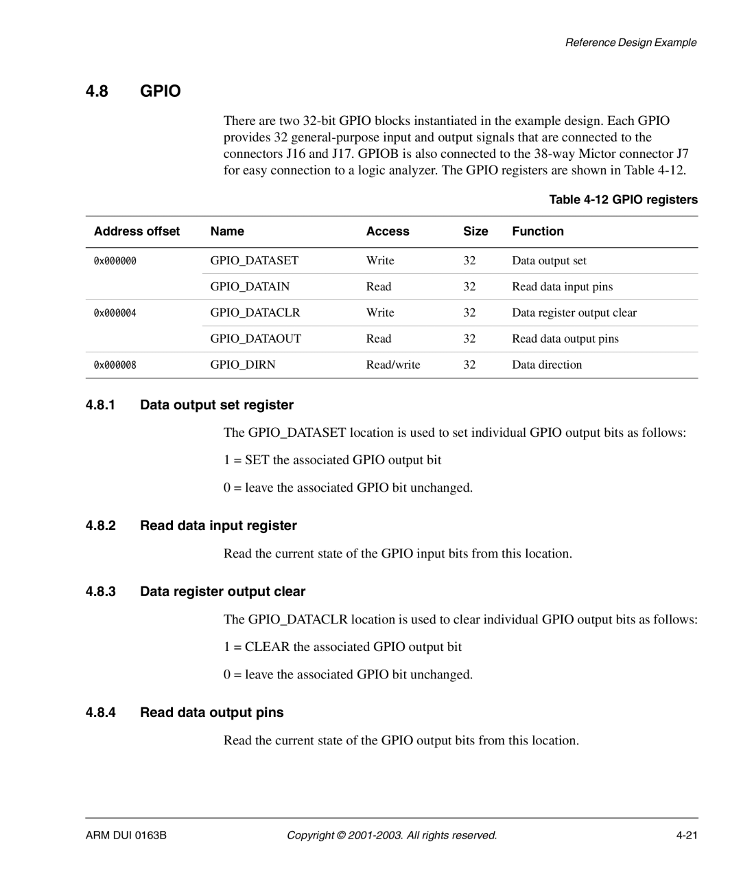
There are two
|
|
|
| Table |
|
|
|
|
|
Address offset | Name | Access | Size | Function |
|
|
|
|
|
0x000000 | GPIO_DATASET | Write | 32 | Data output set |
|
|
|
|
|
| GPIO_DATAIN | Read | 32 | Read data input pins |
|
|
|
|
|
0x000004 | GPIO_DATACLR | Write | 32 | Data register output clear |
|
|
|
|
|
| GPIO_DATAOUT | Read | 32 | Read data output pins |
|
|
|
|
|
0x000008 | GPIO_DIRN | Read/write | 32 | Data direction |
|
|
|
|
|
4.8.1Data output set register
The GPIO_DATASET location is used to set individual GPIO output bits as follows:
1 = SET the associated GPIO output bit
0 = leave the associated GPIO bit unchanged.
4.8.2Read data input register
Read the current state of the GPIO input bits from this location.
4.8.3Data register output clear
The GPIO_DATACLR location is used to clear individual GPIO output bits as follows:
1 = CLEAR the associated GPIO output bit
0 = leave the associated GPIO bit unchanged.
4.8.4Read data output pins
Read the current state of the GPIO output bits from this location.
ARM DUI 0163B | Copyright © |