Reference Design Example
4.7Stepper motor peripheral
The example design instantiates two stepper controller blocks, each of which has two stepper motor controllers. Stepper A controls the Step 1 and 2 interfaces which are connected to the L298 stepper motor drivers. Stepper B controls the Step 3 and 4 interfaces which are connected at logic level to the connectors J21 and J22.
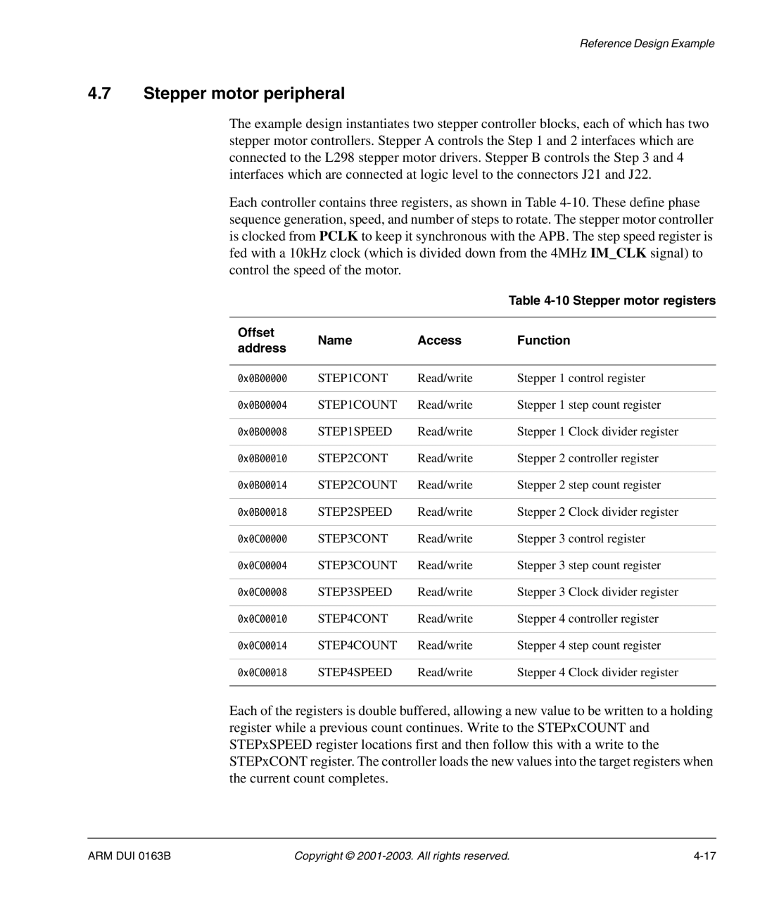
Each controller contains three registers, as shown in Table
|
|
| Table | |
|
|
|
| |
Offset | Name | Access | Function | |
address | ||||
|
|
| ||
|
|
|
| |
0x0B00000 | STEP1CONT | Read/write | Stepper 1 control register | |
|
|
|
| |
0x0B00004 | STEP1COUNT | Read/write | Stepper 1 step count register | |
|
|
|
| |
0x0B00008 | STEP1SPEED | Read/write | Stepper 1 Clock divider register | |
|
|
|
| |
0x0B00010 | STEP2CONT | Read/write | Stepper 2 controller register | |
|
|
|
| |
0x0B00014 | STEP2COUNT | Read/write | Stepper 2 step count register | |
|
|
|
| |
0x0B00018 | STEP2SPEED | Read/write | Stepper 2 Clock divider register | |
|
|
|
| |
0x0C00000 | STEP3CONT | Read/write | Stepper 3 control register | |
|
|
|
| |
0x0C00004 | STEP3COUNT | Read/write | Stepper 3 step count register | |
|
|
|
| |
0x0C00008 | STEP3SPEED | Read/write | Stepper 3 Clock divider register | |
|
|
|
| |
0x0C00010 | STEP4CONT | Read/write | Stepper 4 controller register | |
|
|
|
| |
0x0C00014 | STEP4COUNT | Read/write | Stepper 4 step count register | |
|
|
|
| |
0x0C00018 | STEP4SPEED | Read/write | Stepper 4 Clock divider register | |
|
|
|
|
Each of the registers is double buffered, allowing a new value to be written to a holding register while a previous count continues. Write to the STEPxCOUNT and STEPxSPEED register locations first and then follow this with a write to the STEPxCONT register. The controller loads the new values into the target registers when the current count completes.
ARM DUI 0163B | Copyright © |