Reference Design Example
|
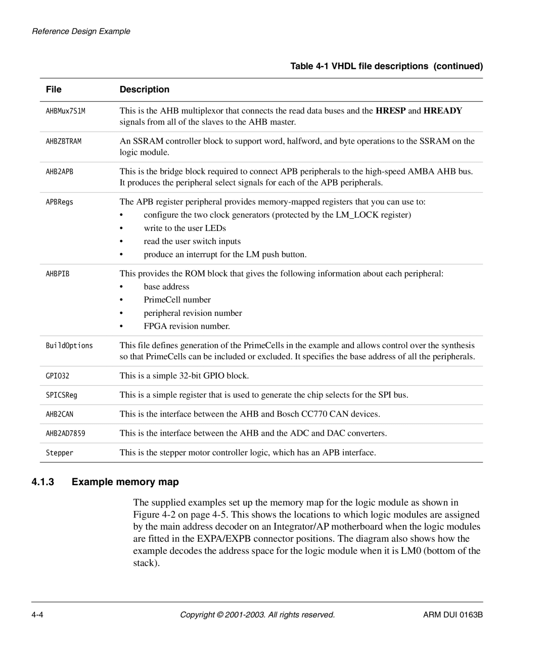
| Table |
|
| |
File | Description | |
|
| |
AHBMux7S1M | This is the AHB multiplexor that connects the read data buses and the HRESP and HREADY | |
| signals from all of the slaves to the AHB master. | |
|
| |
AHBZBTRAM | An SSRAM controller block to support word, halfword, and byte operations to the SSRAM on the | |
| logic module. | |
|
| |
AHB2APB | This is the bridge block required to connect APB peripherals to the | |
| It produces the peripheral select signals for each of the APB peripherals. | |
|
| |
APBRegs | The APB register peripheral provides | |
| • | configure the two clock generators (protected by the LM_LOCK register) |
| • | write to the user LEDs |
| • | read the user switch inputs |
| • | produce an interrupt for the LM push button. |
|
| |
AHBPIB | This provides the ROM block that gives the following information about each peripheral: | |
| • | base address |
| • | PrimeCell number |
| • | peripheral revision number |
| • | FPGA revision number. |
|
| |
BuildOptions | This file defines generation of the PrimeCells in the example and allows control over the synthesis | |
| so that PrimeCells can be included or excluded. It specifies the base address of all the peripherals. | |
|
| |
GPIO32 | This is a simple | |
|
| |
SPICSReg | This is a simple register that is used to generate the chip selects for the SPI bus. | |
|
| |
AHB2CAN | This is the interface between the AHB and Bosch CC770 CAN devices. | |
|
| |
AHB2AD7859 | This is the interface between the AHB and the ADC and DAC converters. | |
|
| |
Stepper | This is the stepper motor controller logic, which has an APB interface. | |
|
|
|
4.1.3Example memory map
The supplied examples set up the memory map for the logic module as shown in Figure
Copyright © | ARM DUI 0163B |