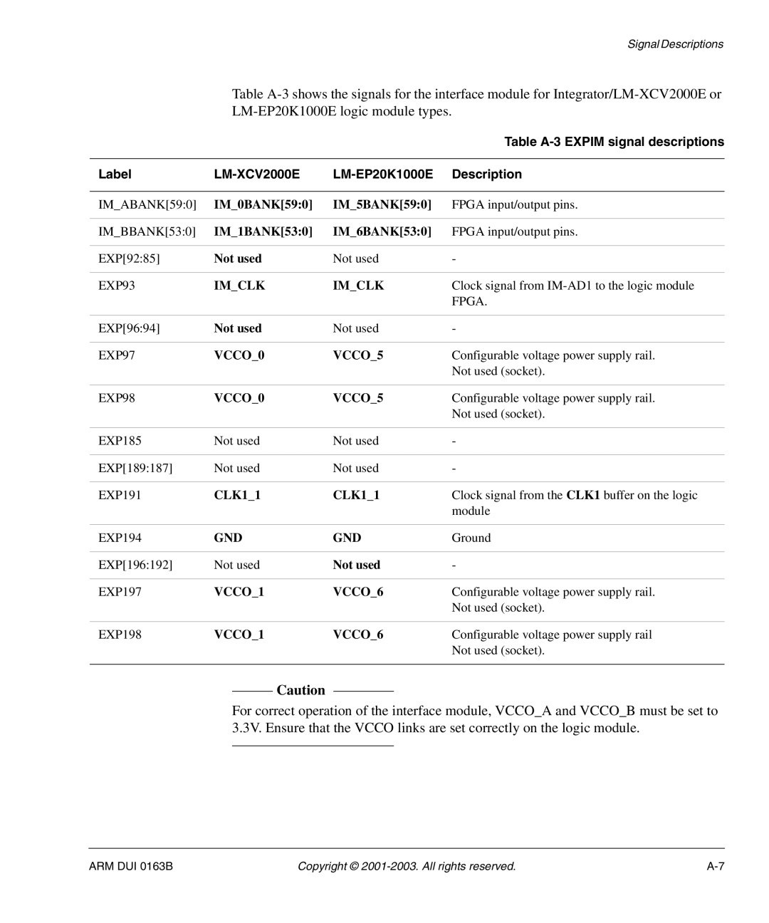
Signal Descriptions
Table
|
|
| Table |
|
|
|
|
Label |
|
| Description |
|
|
|
|
IM_ABANK[59:0] | IM_0BANK[59:0] | IM_5BANK[59:0] | FPGA input/output pins. |
|
|
|
|
IM_BBANK[53:0] | IM_1BANK[53:0] | IM_6BANK[53:0] | FPGA input/output pins. |
|
|
|
|
EXP[92:85] | Not used | Not used | - |
|
|
|
|
EXP93 | IM_CLK | IM_CLK | Clock signal from |
|
|
| FPGA. |
|
|
|
|
EXP[96:94] | Not used | Not used | - |
|
|
|
|
EXP97 | VCCO_0 | VCCO_5 | Configurable voltage power supply rail. |
|
|
| Not used (socket). |
|
|
|
|
EXP98 | VCCO_0 | VCCO_5 | Configurable voltage power supply rail. |
|
|
| Not used (socket). |
|
|
|
|
EXP185 | Not used | Not used | - |
|
|
|
|
EXP[189:187] | Not used | Not used | - |
|
|
|
|
EXP191 | CLK1_1 | CLK1_1 | Clock signal from the CLK1 buffer on the logic |
|
|
| module |
|
|
|
|
EXP194 | GND | GND | Ground |
|
|
|
|
EXP[196:192] | Not used | Not used | - |
|
|
|
|
EXP197 | VCCO_1 | VCCO_6 | Configurable voltage power supply rail. |
|
|
| Not used (socket). |
|
|
|
|
EXP198 | VCCO_1 | VCCO_6 | Configurable voltage power supply rail |
|
|
| Not used (socket). |
|
|
|
|
Caution
For correct operation of the interface module, VCCO_A and VCCO_B must be set to 3.3V. Ensure that the VCCO links are set correctly on the logic module.
ARM DUI 0163B | Copyright © |