By Galil Motion Control, Inc
DMC-2x00
Using This Manual
Contents
Connecting Hardware
Communication
Iv Contents DMC-2X00
Application Programming
Troubleshooting 130
Contents y
Index 210
Overview
DMC- 2000 Family Part Number Definition
Specifications
Electrical Specifications
Mechanical Specifications
Overview of Motor Types
Environmental Specifications
Equipment Maintenance
Standard Servo Motor with +/- 10 Volt Command Signal
Overview of Amplifiers
Stepper Motor with Step and Direction Signals
Amplifiers in Current Mode
Amplifiers in Velocity Mode
Communication
DMC-2x00 Functional Elements
Microcomputer Section
Motor Interface
Amplifier Driver
General I/O
System Elements
Motor
Encoder
Watch Dog Timer
This page Left Blank Intentionally
Getting Started
Outline of the DMC-2000 Daughter Board
DMC-2000 Daughter Board
3B Outline of the DMC-2200 Daughter Board
DMC-2200 Daughter Board
CABLE-USB-2M CABLE-USB-3M
Elements You Need
Recommended System Elements of DMC-2100/DMC-2200
Determine Overall Motor Configuration
Installing the DMC-2x00
Standard Servo Motor Operation
Stepper Motor Operation
Install Jumpers on the DMC-2x00
Master Reset and Upgrade Jumpers
Sinusoidal Commutation
Configure DIP switches on the DMC-2000
Configure DIP switches on the DMC-2200
Switch 4, 5 and 6 Main Serial Port Baud Rate
Switch 10 USB
Configure DIP switches on the DMC-2100
Connect AC Power to the Controller
Install the Communications Software
Communicating through the Main Serial Communications Port
Establish Communications with Galil Software
Communicating through the Ethernet
Communicating through the Universal Serial Bus USB
Determine the Axes to be Used for Sinusoidal Commutation
Sending Test Commands to the Terminal
Make Connections to Amplifier and Encoder
DMC-2X00
Connect Standard Servo Motors
BGA CR
Inverting the Loop Polarity
ICM-2900
Connect Sinusoidal Commutation Motors
Example Sinusoidal Commutation Configuration using a DMC
Getting Started DMC-2X00
SHA
Tune the Servo System
Connect Step Motors
Instruction Interpretation
Design Examples
System Set-up
InstructionInterpretation
Position Interrogation
Profiled Move
Multiple Axes
Independent Moves
Velocity Control
Absolute Position
Interrogation
Operation in the Buffer Mode
Using the On-Board Editor
Operation Under Torque Limit
Motion Programs with Trippoints
Motion Programs with Loops
Line # Instruction Interpretation
AMA
Control Variables
Linear Interpolation
XQ #B
VM AB
Circular Interpolation
LM ABC
BGS
This page Left Blank Intentionally
Limit Switch Input
Using Optoisolated Inputs
Overview
Abort Input
Home Switch Input
Opto-Isolation Common Point
Wiring the Opto-Isolated Inputs
Reset Input
Uncommitted Digital Inputs
Optoisolated Inputs
Using an Isolated Power Supply
Amplifier Interface
Analog Inputs
Bypassing the Opto-Isolation
Auxiliary Encoder Inputs
TTL Inputs
General Use Outputs
TTL Outputs
Output Compare
Extended I/O of the DMC-2x00 Controller
Error Output
Interfacing to Grayhill or OPTO-22 G4PB24
RS232 Auxiliary Port P2 Dataset
Introduction
RS232 Ports
RS232 Main Port P1 Dataterm
Baud Rate Selection
RS-232 Configuration
RS422 Main Port P1
RS422 Auxiliary Port P2
Address
Daisy-Chaining DMC-2000 only
Command Interpretation
Ethernet Configuration DMC-2100/2200 only
Communication Protocols
LED
Addressing
DMC-2X00
Communicating with Multiple Devices
Multicasting
Using Third Party Software
Data Record Map
Data Record
DMC-2X00
BIT
Header Information Byte 0, 1 of Header
Axis Status Information 2 Byte
Axis Switch Information 1 Byte
Bytes 2, 3 of Header
General Status Information 1 Byte
QZ Command
Controller Response to Commands
Galil Software Tools and Libraries
Unsolicited Messages Generated by Controller
Important All DMC-2x00 commands are sent in upper case
Command Syntax Ascii
BG S
BG Abcd
BG Abcdefgh
BG D
Header Format
Command Syntax Binary
LE, VE
Binary Command Table
Datafields Format
Example
Controller Response to Data
Interrogating the Controller
Interrogation Commands
Summary of Interrogation Commands
Interrogating Current Commanded Values
=TPA
Command Summary
This page Left Blank Intentionally
Example Application Mode of Motion Commands
GP, GR
Independent Axis Positioning
VS,VA,VD
GA, GD
Operand Summary Independent Axis
Command Summary Independent Axis
Absolute Position Movement
Examples
Multiple Move Sequence
5000 Time ms 100
Position Tracking
20000
15000 10000
Example Motion
Command Description PT1
Motion
Example
Position vs. Time msec Motion
Velocity vs.Time Motion
Velocity cts/sec vs. Time msec with IT Motion
Trip Points
Command Summary Jogging
Command Summary Position Tracking Mode
Independent Jogging
#JOY
Jog in X only
Joystick Jogging
AS a
Specifying the Coordinate Plane
Linear Interpolation Mode
Specifying Linear Segments
#ALT
Additional Commands
Specifying Vector Speed for Each Segment
Changing Feed Rate
Operand Summary Linear Interpolation
Command Summary Linear Interpolation
Linear Interpolation Motion
LM CD
Linear Move
Position D
Multiple Moves
Vector Mode Linear and Circular Interpolation Motion
Specifying Vector Segments
Tangent Motion
Compensating for Differences in Encoder Resolution
Command Summary Coordinated Motion Sequence
Trippoints
Tangent Axis
Operand Summary Coordinated Motion Sequence
Operand
SB0
Coordinated Motion
BG ABC
AM ABC
Ramped Gearing
Electronic Gearing
Velocity cts/sec vs. Time msec Ramped Gearing
GA Z, Z
Command Summary Electronic Gearing
Electronic Gearing Over a Specified Interval
MO Z
Simple Master/Slave
Gantry Mode
Electronic Gearing
GA,A
Electronic Cam
DMC-2X00
3000 2250 1500 2000 4000 6000 Master a
Command Description
Command Summary Electronic CAM
Electronic CAM
Operand Summary Electronic CAM
Specifying Contour Segments
Contour Mode
CMA
336 288 240 192 Time ms
DT0CD0
Generating an Array
Command Summary Contour Mode
Command Description CM Abcdefgh
General Velocity Profiles
#POINTS
Contour Mode
Record and Playback Example
Teach Record and Play-Back
Ecam master example
Virtual Axis
Sinusoidal Motion Example
Stepper Motor Smoothing
Monitoring Generated Pulses vs. Commanded Pulses
Stepper Motor Operation
Specifying Stepper Motor Operation
Command Summary Stepper Motor Operation
Using an Encoder with Stepper Motors
Motion Complete Trip point
Operand Summary Stepper Motor Operation
Stepper Position Maintenance Mode SPM
SHX
Error Limit
Example SPM Mode Setup
Correction
#MOTION
Example Error Correction
Example Friction Correction
Dual Loop Auxiliary Encoder
= Main Encoder Second Encoder
Additional Commands for the Auxiliary Encoder
Backlash Compensation
Continuous Dual Loop
DE0
Motion Smoothing
Sampled Dual Loop
#DUALOOP
Using the IT and VT Commands
Trapezoidal velocity and smooth velocity profiles
Using the KS Command Step Motor Smoothing
Homing
Home Sensor Home Switch
Input Function
Command Summary Homing Operation
High Speed Position Capture The Latch Function
Operand Summary Homing Operation
JP #WAIT,ALB=1
#LATCH
AL B
#WAIT
Application Programming
Using the DOS Editor to Enter Programs DMC-2000 only
ED #BEGIN
Edit Mode Commands
#START
Using Labels in Programs
Program Format
Special Labels
Commenting Programs
No Command
Executing Programs Multitasking
REM Command
REM Half Circle Motion VP 0,3000 REM TOP Line
Debugging Programs
Trace Commands DMC-2100/2200 only
Stop Code Command
Error Code Command
RAM Memory Interrogation Commands
Event Triggers & Trippoints
Program Flow Commands
DMC-2x00 Event Triggers
Command Function
AS a B C D E F G H
Example Start Motion on Input
Example- Multiple Move Sequence
Example- Set Output after Distance
Example- Repetitive Position Trigger
Example Change Speed along Vector Path
Example Set Output when At Speed
Example Multiple Move with Wait
Example- Define Output Waveform Using AT
Conditional Jumps
Multiple Conditional Statements
Command Format JP and JS
Logical operators
Conditional Statements
#BEGIN
Examples
If, Else, and Endif
JP#A
Nesting if Conditional Statements
Using the if and Endif Commands
Using the Else Command
Command Format IF, Else and Endif
Stack Manipulation
Subroutines
Auto-Start Routine
Automatic Subroutines for Monitoring Conditions
Example Limit Switch
Example Motion Complete Timeout
Example Position Error
Example Input Interrupt
Example Command Error
Example Communication Interrupt
Example Command Error w/Multitasking
PAA=0
Example Ethernet Communication Error
Operator Function
Mathematical and Functional Expressions
Mathematical Operators
Bit-Wise Operators
Response from command MG len6 S4
Functions
Variables
Assigning Values to Variables
Programmable Variables
Assigning Variable Values to Controller Parameters
Special Operands Keywords
Example Using Variables for Joystick
Operands
Displaying the value of variables at the terminal
Time
Arrays
Defining Arrays
Assignment of Array Entries
Uploading and Downloading Arrays to On Board Memory
Using a Variable to Address Array Elements
Automatic Data Capture into Arrays
Example Recording into an Array
Command Summary Automatic Data Capture
Data Types for Recording
Operand Summary Automatic Data Capture
Example- Inputting Numeric Data
Input of Data Numeric and String
Deallocating Array Space
Input of Data
Keyword Function
Operator Data Entry Mode
Using Communication Interrupt
Inputting String Variables
Output of Data Numeric and String
Specifying the Port for Messages
Sending Messages
Formatting Messages
Example Printing a Variable and an Array element
Using the MG Command to Configure Terminals
Summary of Message Functions
Displaying Variables and Arrays
LZ0
0000000009
LZ1
Local Formatting of Response of Interrogation Commands
Formatting Variables and Array Elements
Local Formatting of Variables
Alph
Hardware I/O
Converting to User Units
Digital Outputs
Example Turn on output after move
Example- Set Bit and Clear Bit
Example- Output Bit
Example- Output Port
AI 1BGA
Example Using Inputs to control program flow
Example Start Motion on Switch
Input Interrupt Function
ST AB
Analog Inputs
Example Position Follower Point-to-Point
TP AB
#CONT
Configuring the I/O of the DMC-2x00
Example Position Follower Continuous Move
PA VP
Argument Blocks Bits Description
Accessing Extended I/O
Saving the State of the Outputs in Non-Volatile Memory
Bit I/O Block Binary Decimal Value for Representation
Example Applications
Wire Cutter
Interfacing to Grayhill or OPTO-22 G4PB24
JP #A
Table Controller
BGC AMC
AMC
BGS AMS
Speed Control by Joystick
Backlash Compensation by Sampled Dual-Loop
Position Control by Joystick
BGA JP #B
This page Left Blank Intentionally
Output Protection Lines
Hardware Protection
Input Protection Lines
Software Protection
#AJP #AEN
Off-On-Error
Automatic Error Routine
Programmable Position Limits
Limit Switch Routine
Installation
Troubleshooting
Stability
Communication
Operation
Theory of Operation
Level
Velocity and Position Profiles
Operation of Closed-Loop Systems
Functional Elements of a Motion Control System
System Modeling
Voltage Drive
Motor-Amplifier
Current Drive
Elements of velocity loops
Velocity Loop
Voltage Source
Digital Filter
DAC
ZOH
System Analysis
Magnitude 200 2000 Rad/s
Analytical Method
System Design and Compensation
Theory of Operation DMC-2X00
Equivalent Filter Form
Input / Output
Electrical Specifications
Servo Control
Stepper Control
Normal
Performance Specifications
Power
Minimum Servo Loop Update Time
Fast Update Rate Mode
DMC-2x00 Axes A-D High Density Connector
Connectors for DMC-2x00 Main Board
DMC-2x00 Axes E-H High Density Connector
DMC-2x00 Extended I/O 80 Pin High Density Connector
DMC-2x00 Auxiliary Encoder 36 Pin High Density Connector
+5V
USB USB Out
Pin Signal
RS-232-Main Port
RS-232-Auxiliary Port
Ethernet
Standard RS-232 Specifications
Pin Serial Connector Male, D-type
Cable Connections for DMC-2x00
Pin Male computer Pin female controller
DMC-2x00 Serial Cable Specifications
Pin Male terminal Pin male controller
Pin Female Computer Pin Female Controller
Pin Female terminal Pin Male Controller
Outputs
Pin-Out Description for DMC-2x00
Inputs
Appendices DMC-2X00
Jumper Label
Jumper Description for DMC-2x00
Function If jumpered
Dimensions for DMC-2x00
DMCWIN16 DMCWIN32 SETUP16 SETUP32 KIT
Accessories and Options
Description
ICM-2900 Interconnect Module
Block 4 PIN Label Description
Signy
Error
Pwmx
Mocmdy
Ylatch
Reset
IN8
Xlatch
MBZ
+MAZ
MAZ
+MBZ
ICM
ICM-2900 Drawing
ICM-2908 Interconnect Module
ICM-2908
ICM-2908 Drawing
PCB Layout of the ICM-2900
Terminal Label
Features
ISO OUT Power Error Reset CMP Mocmdw
ICM-1900 Interconnect Module
DMC-2X00
100 101 102 103 104 105 106 107
ICM-1900 Drawing
AMP-19x0 Mating Power Amplifiers
MBW +INW
Opto-Isolated Outputs for ICM-2900 / ICM-1900 / AMP
Specifications
Standard Opto-Isolation and High Current Opto-isolation
DMC-2000 ICM-1900 / ICM-2900
Configuring the Amplifier Enable for ICM-2900 / ICM
Changing the Amplifier Enable Voltage Level
Laen Option
Overview
IOM-1964 Opto-Isolation Module for Extended I/O
Figure A-7
Configuring Hardware Banks
Input Circuit
Figure A-10
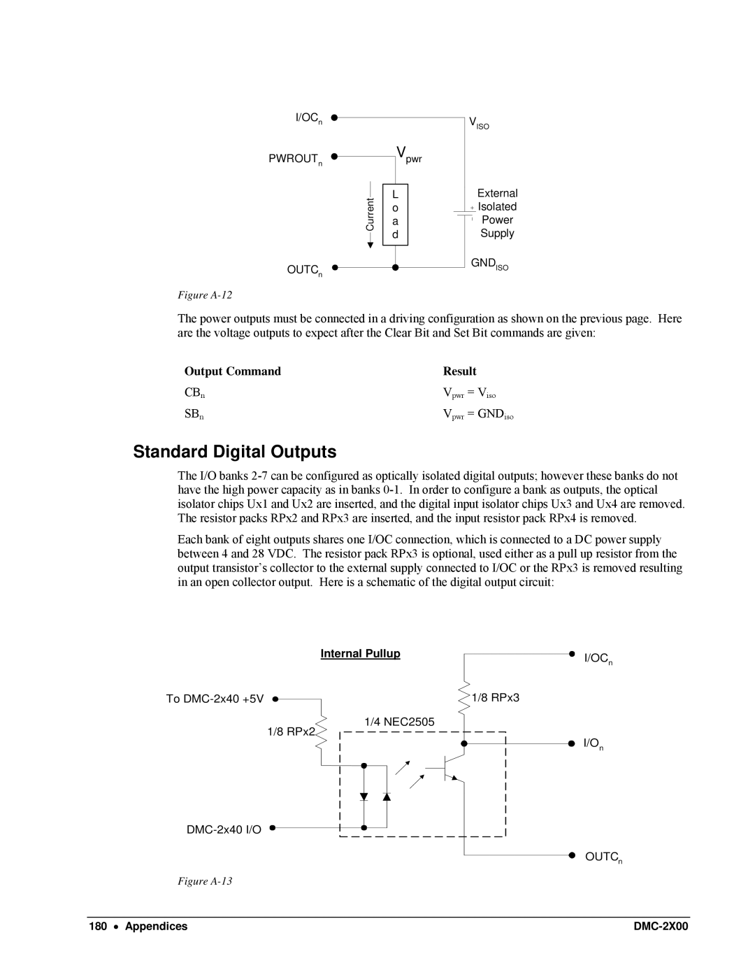
High Power Digital Outputs
Figure A-12
Standard Digital Outputs
Figure A-14
Digital Inputs
Screw Terminal Listing
High Power Digital Outputs
Relevant DMC Commands
Standard Digital Outputs
DMC-2X00
PWROUT29
PWROUT32
PWROUT31
PWROUT30
CB-50-100 Adapter Board
Connectors
Appendices DMC-2X00
JC6 50 PIN IDC J9 100 PIN High Density Connector
JC8 JC6
CB-50-100 Drawing
Figure A-16
CB-50-80 Adapter Board
JC8
JC6
CB-50-80 Outline
CB-50-80 Drawing
CB-50-80 Layout
Figure A-19
TERM-1500 Operator Terminal
Figure A-20
Specifications Hand-Held
Shift Key Output
Specifications Panel Mount
Keypad Maps Hand-Held
Single Key Output
Cursor Movement Commands
Escape Commands
Keypad Map Panel Mount 6 columns x 5 rows
Configuration
Function Keys
Default Configuration
Default Function Keys
Input/Output of Data DMC-2x00 Commands
Pin D Adaptor Male For P2
Pin Modular Connector
Ordering Information
Vs = Vx 2 + Vy
Coordinated Motion Mathematical Analysis
Lk = Xk 2 + Yk
Velocity
Example- Communicating with OPTO-22 SNAP-B3000
NUMOFIO=4
#CFGDOUT
MODULE=2
CFGVALUE=$180
Appendices DMC-2X00
DMC-2x00 DMC-1500
DMC-2x00/DMC-1500 Comparison
Training Seminars
List of Other Publications
Contacting Us
Warranty
Limswi
Index
PID
Poserr