Hardware Design
•Do not place
•Arrange the board so that return currents for
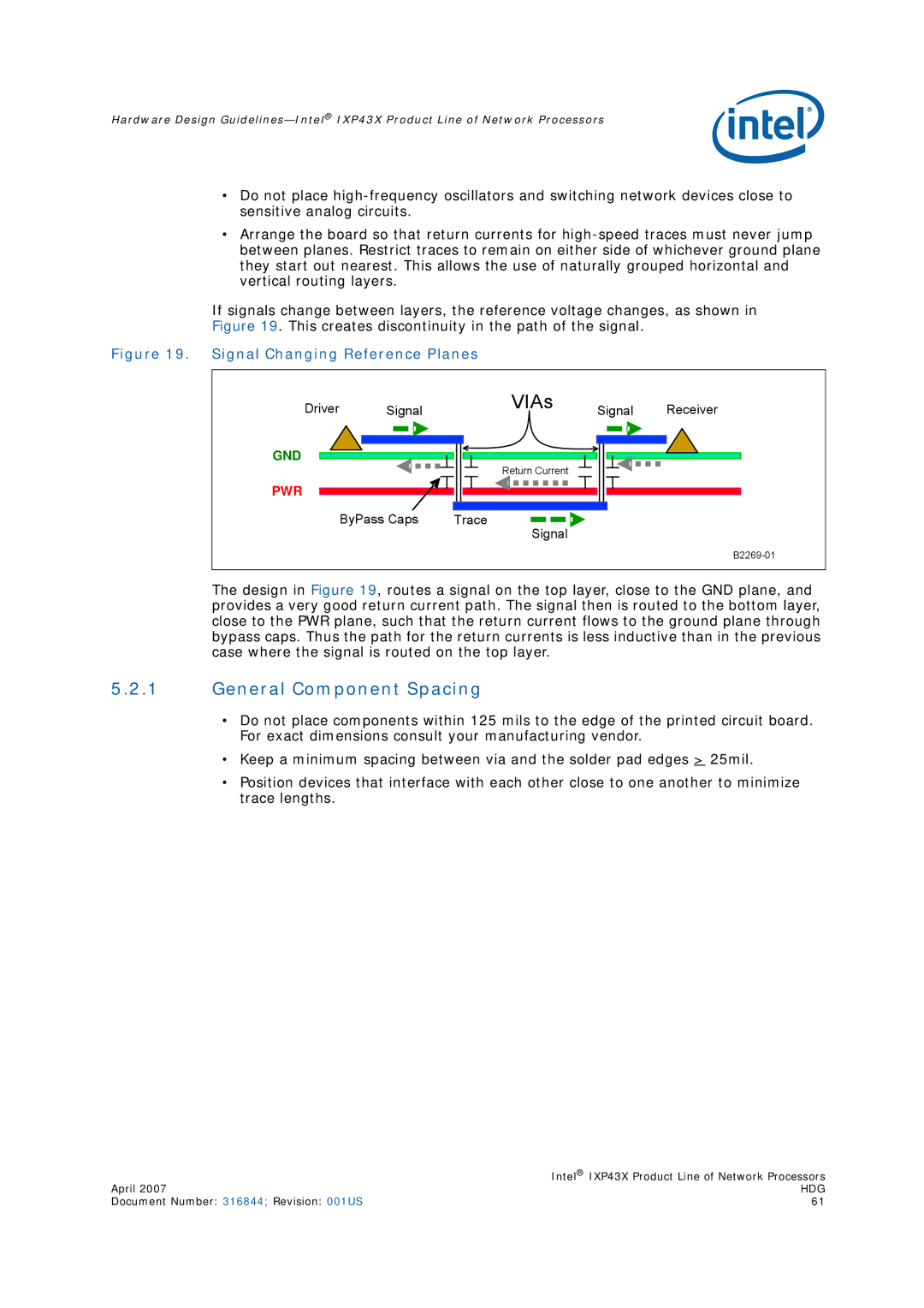
If signals change between layers, the reference voltage changes, as shown in Figure 19. This creates discontinuity in the path of the signal.
Figure 19. Signal Changing Reference Planes
Driver Signal
VIAs
Signal Receiver
GND
Return Current
PWR
ByPass Caps | Trace |
Signal
The design in Figure 19, routes a signal on the top layer, close to the GND plane, and provides a very good return current path. The signal then is routed to the bottom layer, close to the PWR plane, such that the return current flows to the ground plane through bypass caps. Thus the path for the return currents is less inductive than in the previous case where the signal is routed on the top layer.
5.2.1General Component Spacing
•Do not place components within 125 mils to the edge of the printed circuit board. For exact dimensions consult your manufacturing vendor.
•Keep a minimum spacing between via and the solder pad edges > 25mil.
•Position devices that interface with each other close to one another to minimize trace lengths.
| Intel® IXP43X Product Line of Network Processors |
April 2007 | HDG |
Document Number: 316844; Revision: 001US | 61 |