Hardware Design
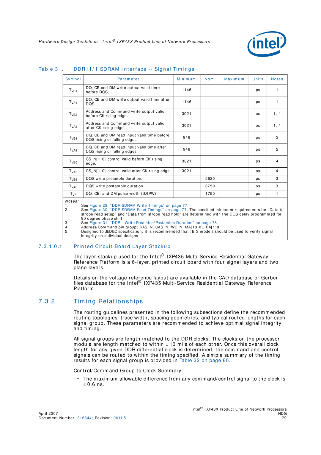
Table 31. | DDR II/I SDRAM Interface |
|
|
|
|
| ||||
|
|
|
|
|
|
|
|
|
|
|
|
| Symbol |
| Parameter | Minimum | Nom. |
| Maximum | Units | Notes |
|
|
|
|
|
|
|
|
|
|
|
|
| TVB1 |
| DQ, CB and DM write output valid time | 1146 |
|
|
| ps | 1 |
|
|
| before DQS. |
|
|
| ||||
|
| TVA1 |
| DQ, CB and DM write output valid time after | 1146 |
|
|
| ps | 1 |
|
|
| DQS. |
|
|
| ||||
|
| TVB3 |
| Address and Command write output valid | 3021 |
|
|
| ps | 1, 4 |
|
|
| before CK rising edge. |
|
|
| ||||
|
| TVA3 |
| Address and Command write output valid | 3021 |
|
|
| ps | 1, 4 |
|
|
| after CK rising edge. |
|
|
| ||||
|
| TVB4 |
| DQ, CB and DM read input valid time before | 948 |
|
|
| ps | 2 |
|
|
| DQS rising or falling edges. |
|
|
| ||||
|
| TVA4 |
| DQ, CB and DM read input valid time after | 948 |
|
|
| ps | 2 |
|
|
| DQS rising or falling edges. |
|
|
| ||||
|
| TVB5 |
| CS_N[1:0] control valid before CK rising | 3021 |
|
|
| ps | 4 |
|
|
| edge. |
|
|
| ||||
|
| TVA5 |
| CS_N[1:0] control valid after CK rising edge. | 3021 |
|
|
| ps | 4 |
|
| TVB6 |
| DQS write preamble duration. |
| 5625 |
|
| ps | 3 |
|
| TVA6 |
| DQS write postamble duration. |
| 3750 |
|
| ps | 3 |
|
| TV7 |
| DQ, CB, and DM pulse width (tDIPW) |
| 1750 |
|
| ps | 1 |
|
| Notes: |
|
|
|
|
|
|
|
|
|
| 1. | See Figure 29, “DDR SDRAM Write Timings” on page 77 |
|
|
|
|
| ||
|
| 2. | See Figure 30, “DDR SDRAM Read Timings” on page 77. The specified minimum requirements for “Data to | |||||||
|
|
| strobe read setup” and “Data from strobe read hold” are determined with the DQS delay programmed for | |||||||
|
|
| 90 degree phase shift. |
|
|
|
|
|
| |
|
| 3. | See Figure 31, “DDR - Write Preamble/Postamble Duration” on page 78 |
|
|
| ||||
|
| 4. | Address/Command pin group; RAS_N, CAS_N, WE_N, MA[13:0], BA[1:0] |
|
|
| ||||
|
| 5. | Designed to JEDEC specification; it is recommended that IBIS models should be used to verify signal | |||||||
|
|
| integrity on individual designs |
|
|
|
|
|
| |
|
|
|
|
|
|
|
|
|
|
|
7.3.1.0.1Printed Circuit Board Layer Stackup
The layer stackup used for the Intel® IXP435
Details on the voltage reference layout are available in the CAD database or Gerber files database for the Intel® IXP435
7.3.2Timing Relationships
The routing guidelines presented in the following subsections define the recommended routing topologies, trace width, spacing geometries, and typical routed lengths for each signal group. These parameters are recommended to achieve optimal signal integrity and timing.
All signal groups are length matched to the DDR clocks. The clocks on the processor module are length matched to within ±10 mils of each other. Once this overall clock length for any given DDR differential clock is determined, the command and control signals can be routed to within the timing specified. A simple summary of the timing results for each signal group is provided in Table 32 on page 80.
Control/Command Group to Clock Summary:
•The maximum allowable difference from any command/control signal to the clock is ±0.6 ns.
| Intel® IXP43X Product Line of Network Processors |
April 2007 | HDG |
Document Number: 316844; Revision: 001US | 79 |