Hardware Design
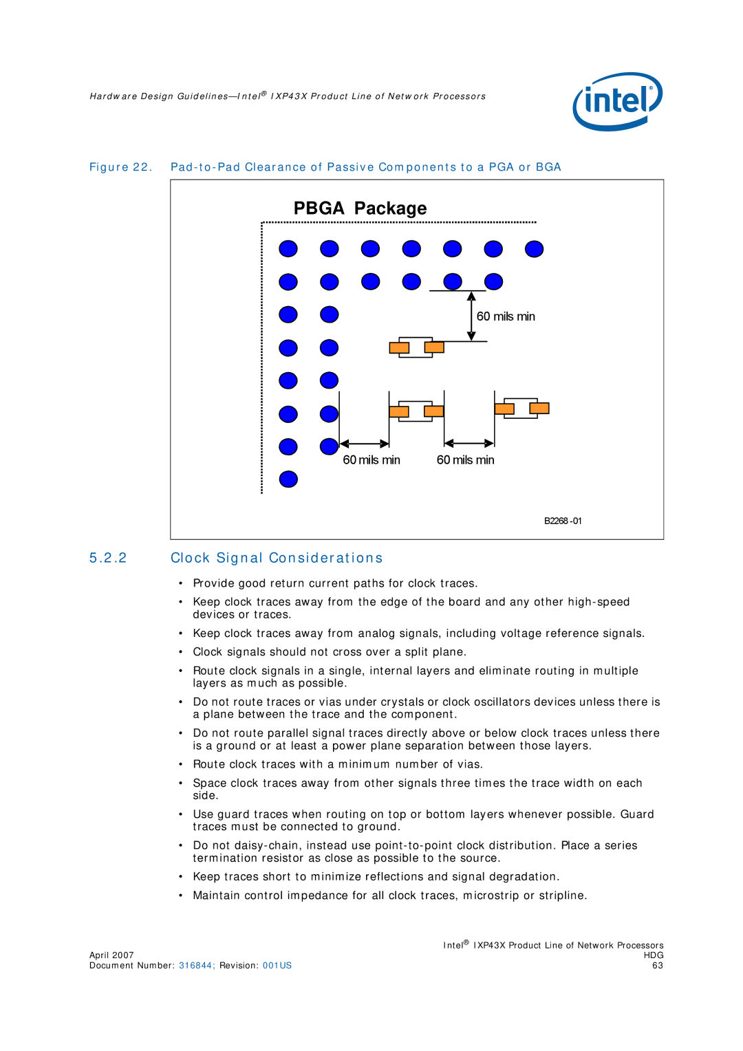
Figure 22. Pad-to-Pad Clearance of Passive Components to a PGA or BGA
PBGA Package
60 mils min
60 mils min | 60 mils min |
B2268
5.2.2Clock Signal Considerations
•Provide good return current paths for clock traces.
•Keep clock traces away from the edge of the board and any other
•Keep clock traces away from analog signals, including voltage reference signals.
•Clock signals should not cross over a split plane.
•Route clock signals in a single, internal layers and eliminate routing in multiple layers as much as possible.
•Do not route traces or vias under crystals or clock oscillators devices unless there is a plane between the trace and the component.
•Do not route parallel signal traces directly above or below clock traces unless there is a ground or at least a power plane separation between those layers.
•Route clock traces with a minimum number of vias.
•Space clock traces away from other signals three times the trace width on each side.
•Use guard traces when routing on top or bottom layers whenever possible. Guard traces must be connected to ground.
•Do not
•Keep traces short to minimize reflections and signal degradation.
•Maintain control impedance for all clock traces, microstrip or stripline.
| Intel® IXP43X Product Line of Network Processors |
April 2007 | HDG |
Document Number: 316844; Revision: 001US | 63 |