Hardware Design
Table 28. | Supported DDRII |
|
|
| |||||
|
|
|
|
|
|
|
|
|
|
|
|
|
| Address Size | Leaf Select | Total |
| ||
DDR SDRAM |
| DDR SDRAM | # of |
|
|
|
| Page | |
|
|
|
|
| Memory | ||||
Technology |
| Arrangement | Banks |
|
| DDR_BA[1 |
| Size | |
| Row | Column | DDR_BA[0] | Size | |||||
|
|
|
| ] |
| ||||
|
|
|
|
|
|
|
|
| |
|
|
|
|
|
|
|
|
|
|
256 Mbit |
| 16M x16 | 1 | 13 | 9 | ADDR[24] | ADDR[23] | 32MB | 1KB |
|
|
|
|
|
|
|
|
|
|
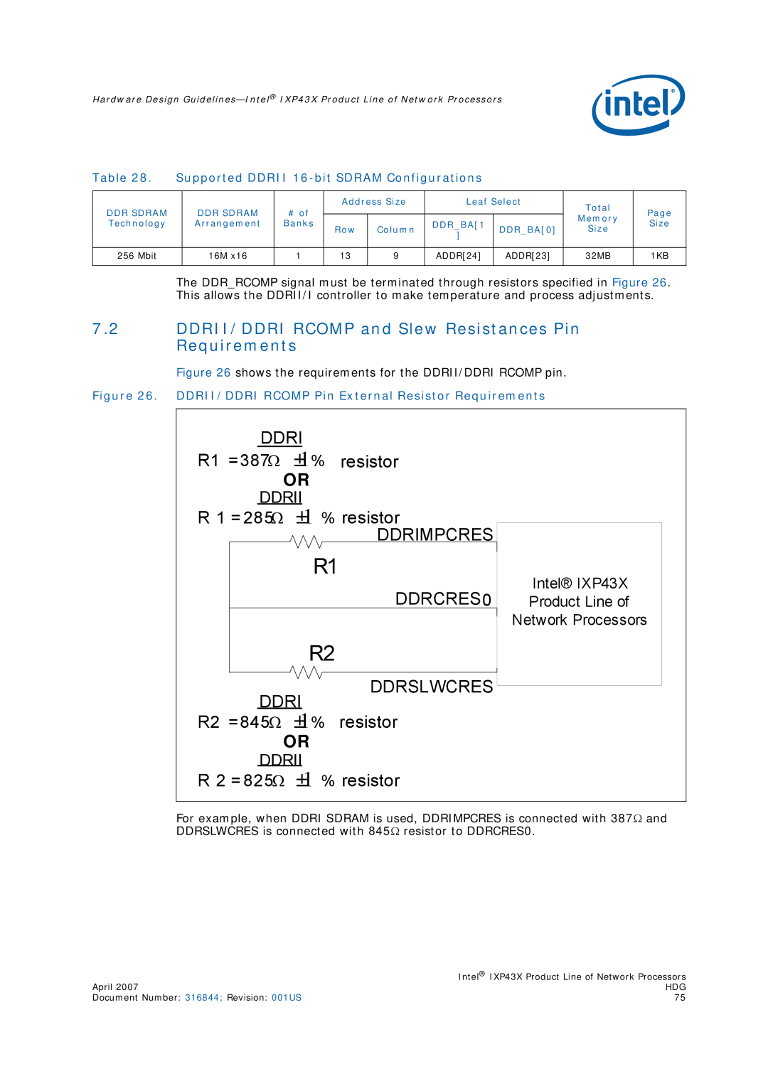
The DDR_RCOMP signal must be terminated through resistors specified in Figure 26. This allows the DDRII/I controller to make temperature and process adjustments.
7.2DDRII/DDRI RCOMP and Slew Resistances Pin Requirements
Figure 26 shows the requirements for the DDRII/DDRI RCOMP pin.
Figure 26. DDRII/DDRI RCOMP Pin External Resistor Requirements
DDRI |
| |
R1 =387Ω ±1% resistor |
| |
OR |
| |
DDRII |
| |
R 1 = 285Ω ±1 % resistor |
| |
DDRIMPCRES |
| |
R1 | Intel® IXP43X | |
DDRCRES0 | ||
Product Line of | ||
| Network Processors | |
R2 |
| |
DDRSLWCRES |
| |
DDRI |
| |
R2 =845Ω ±1% resistor |
| |
OR |
| |
DDRII |
| |
R 2 = 825Ω ±1 % resistor |
|
For example, when DDRI SDRAM is used, DDRIMPCRES is connected with 387Ω and DDRSLWCRES is connected with 845Ω resistor to DDRCRES0.
| Intel® IXP43X Product Line of Network Processors |
April 2007 | HDG |
Document Number: 316844; Revision: 001US | 75 |
