Monaco Technical Reference | Spectrum Signal Processing |
Processor Nodes
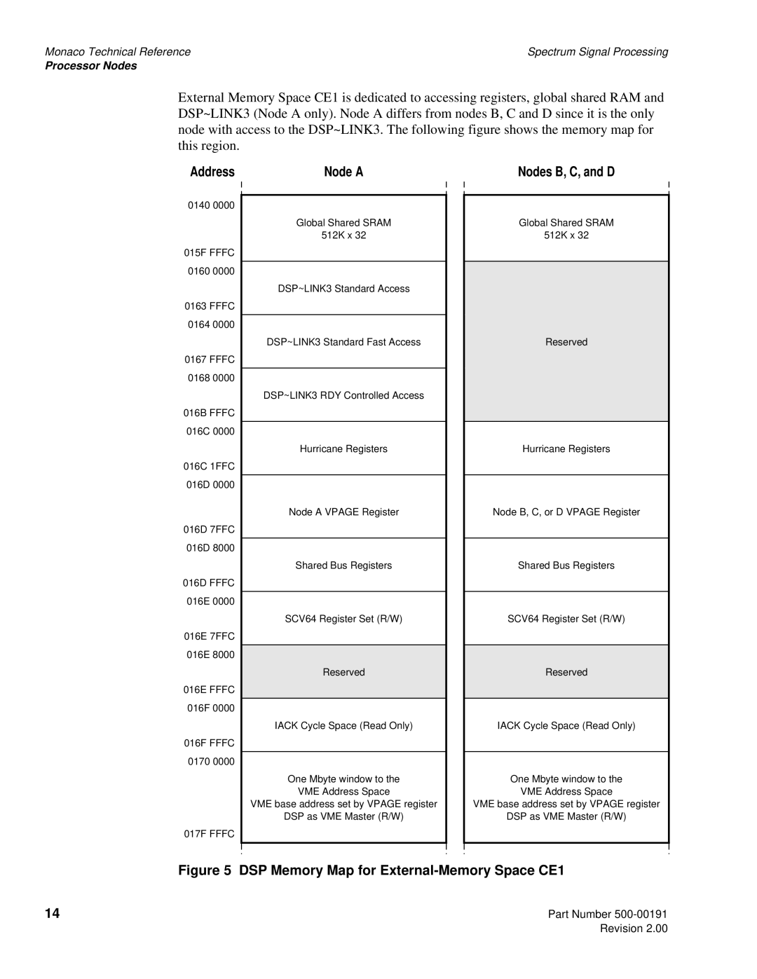
External Memory Space CE1 is dedicated to accessing registers, global shared RAM and DSP~LINK3 (Node A only). Node A differs from nodes B, C and D since it is the only node with access to the DSP~LINK3. The following figure shows the memory map for this region.
Address | Node A |
Nodes B, C, and D
0140 0000
015F FFFC
0160 0000
0163 FFFC
0164 0000
0167 FFFC
0168 0000
016B FFFC
016C 0000
016C 1FFC
016D 0000
016D 7FFC
016D 8000
016D FFFC
016E 0000
016E 7FFC
016E 8000
016E FFFC
016F 0000
016F FFFC
0170 0000
017F FFFC
Global Shared SRAM
512K x 32
DSP~LINK3 Standard Access
DSP~LINK3 Standard Fast Access
DSP~LINK3 RDY Controlled Access
Hurricane Registers
Node A VPAGE Register
Shared Bus Registers
SCV64 Register Set (R/W)
Reserved
IACK Cycle Space (Read Only)
One Mbyte window to the
VME Address Space
VME base address set by VPAGE register
DSP as VME Master (R/W)
Global Shared SRAM
512K x 32
Reserved
Hurricane Registers
Node B, C, or D VPAGE Register
Shared Bus Registers
SCV64 Register Set (R/W)
Reserved
IACK Cycle Space (Read Only)
One Mbyte window to the
VME Address Space
VME base address set by VPAGE register
DSP as VME Master (R/W)
Figure 5 DSP Memory Map for External-Memory Space CE1
14 | Part Number |
| Revision 2.00 |