Monaco Technical Reference | Spectrum Signal Processing |
Processor Nodes
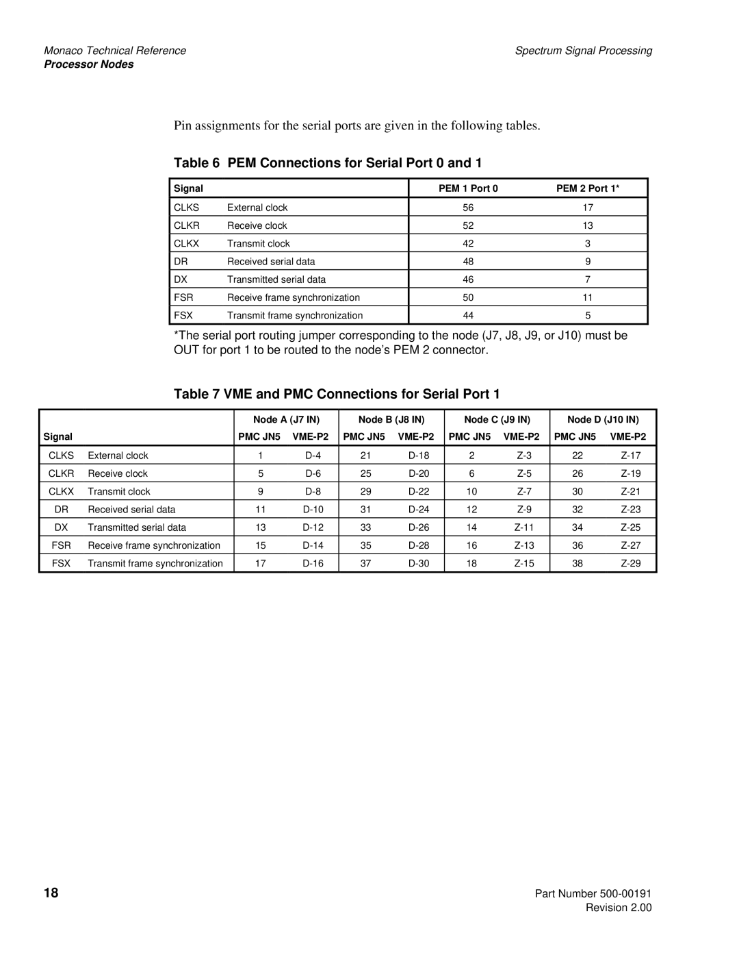
Pin assignments for the serial ports are given in the following tables.
Table 6 PEM Connections for Serial Port 0 and 1
Signal |
| PEM 1 Port 0 | PEM 2 Port 1* |
|
|
|
|
CLKS | External clock | 56 | 17 |
|
|
|
|
CLKR | Receive clock | 52 | 13 |
|
|
|
|
CLKX | Transmit clock | 42 | 3 |
|
|
|
|
DR | Received serial data | 48 | 9 |
|
|
|
|
DX | Transmitted serial data | 46 | 7 |
|
|
|
|
FSR | Receive frame synchronization | 50 | 11 |
|
|
|
|
FSX | Transmit frame synchronization | 44 | 5 |
|
|
|
|
*The serial port routing jumper corresponding to the node (J7, J8, J9, or J10) must be OUT for port 1 to be routed to the node’s PEM 2 connector.
Table 7 VME and PMC Connections for Serial Port 1
|
| Node A (J7 IN) | Node B (J8 IN) | Node C (J9 IN) | Node D (J10 IN) | ||||
Signal |
| PMC JN5 |
| PMC JN5 | PMC JN5 | PMC JN5 | |||
|
|
|
|
|
|
|
|
|
|
CLKS | External clock | 1 | 21 | 2 | 22 | ||||
|
|
|
|
|
|
|
|
|
|
CLKR | Receive clock | 5 | 25 | 6 | 26 | ||||
|
|
|
|
|
|
|
|
|
|
CLKX | Transmit clock | 9 | 29 | 10 | 30 | ||||
|
|
|
|
|
|
|
|
|
|
DR | Received serial data | 11 | 31 | 12 | 32 | ||||
|
|
|
|
|
|
|
|
|
|
DX | Transmitted serial data | 13 | 33 | 14 | 34 | ||||
|
|
|
|
|
|
|
|
|
|
FSR | Receive frame synchronization | 15 | 35 | 16 | 36 | ||||
|
|
|
|
|
|
|
|
|
|
FSX | Transmit frame synchronization | 17 | 37 | 18 | 38 | ||||
|
|
|
|
|
|
|
|
|
|
18 | Part Number |
| Revision 2.00 |