Spectrum Signal Processing | Monaco Technical Reference |
| VME64 Bus Interface |
VME Offset Address
00 0000h
00 0FFFh
00 1000h
00 1003h
00 1004h
00 1007h
00 1008h
00 1FFFh
00 2000h
00 2FFFh
00 3000h
00 3FFFh
00 4000h
00 4FFFh
00 5000h
00 5FFFh
00 6000h
00 FFFFh
01 0000h
01 3FFCh
01 4000h
01 3FFCh
01 B000h
01 3FFCh
01 C000h
01 FFFCh
Test Bus Controller Registers (JTAG)
VME A24 Status Register (Read Only)
VME A24 Control Register (Read/Write)
Reserved
Node A HPI Registers
Node B HPI Registers
Node C HPI Registers
Node D HPI Registers
Reserved
Node A HPID DMA Space (HPIA incremented)
all addresses mapped to 00 2008h
Node B HPID DMA Space (HPIA incremented)
all addresses mapped to 00 3008h
Node C HPID DMA Space (HPIA incremented)
all addresses mapped to 00 4008h
Node D HPID DMA Space (HPIA incremented)
all addresses mapped to 00 5008h
16KB
16KB
16KB
16KB
FPGA
‘C6x
‘C6x
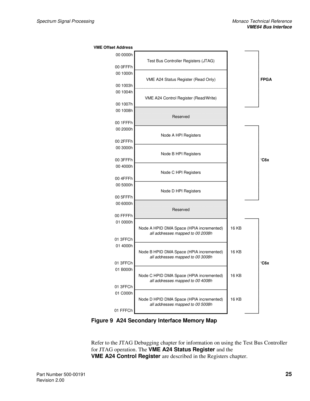
Figure 9 A24 Secondary Interface Memory Map
Refer to the JTAG Debugging chapter for information on using the Test Bus Controller for JTAG operation. The VME A24 Status Register and the
VME A24 Control Register are described in the Registers chapter.
Part Number | 25 |
Revision 2.00 |
|
