Monaco Technical Reference
VME64 Bus Interface
Spectrum Signal Processing
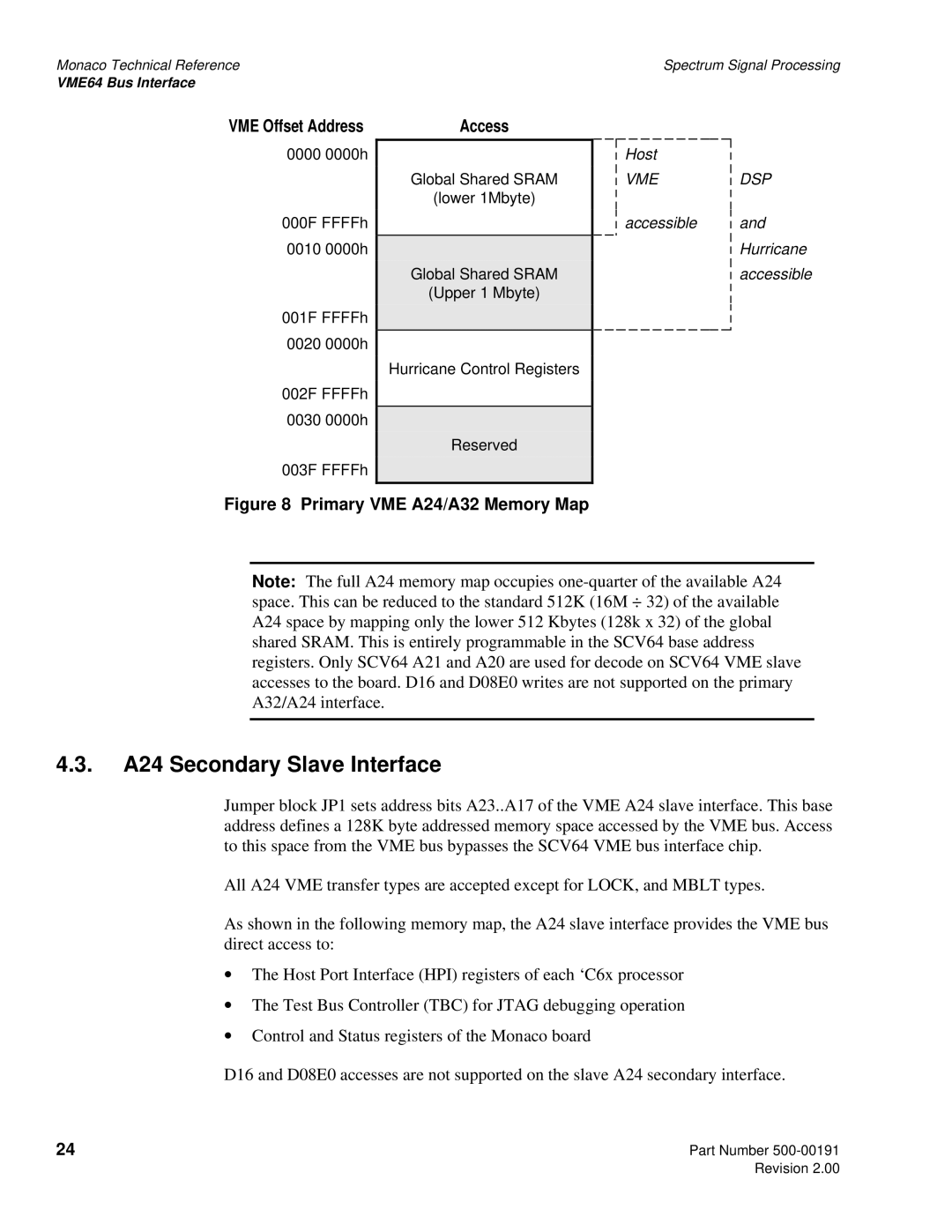
VME Offset Address
0000 0000h
000F FFFFh
0010 0000h
001F FFFFh
0020 0000h
002F FFFFh
0030 0000h
003F FFFFh
Access
Global Shared SRAM
(lower 1Mbyte)
Global Shared SRAM
(Upper 1 Mbyte)
Hurricane Control Registers
Reserved
Host
VMEDSP
accessible and Hurricane accessible
Figure 8 Primary VME A24/A32 Memory Map
Note: The full A24 memory map occupies
4.3.A24 Secondary Slave Interface
Jumper block JP1 sets address bits A23..A17 of the VME A24 slave interface. This base address defines a 128K byte addressed memory space accessed by the VME bus. Access to this space from the VME bus bypasses the SCV64 VME bus interface chip.
All A24 VME transfer types are accepted except for LOCK, and MBLT types.
As shown in the following memory map, the A24 slave interface provides the VME bus direct access to:
∙The Host Port Interface (HPI) registers of each ‘C6x processor
∙The Test Bus Controller (TBC) for JTAG debugging operation
∙Control and Status registers of the Monaco board
D16 and D08E0 accesses are not supported on the slave A24 secondary interface.
24 | Part Number |
| Revision 2.00 |