TMS320C6727, TMS320C6726, TMS320C6722
www.ti.com
SPRS268E
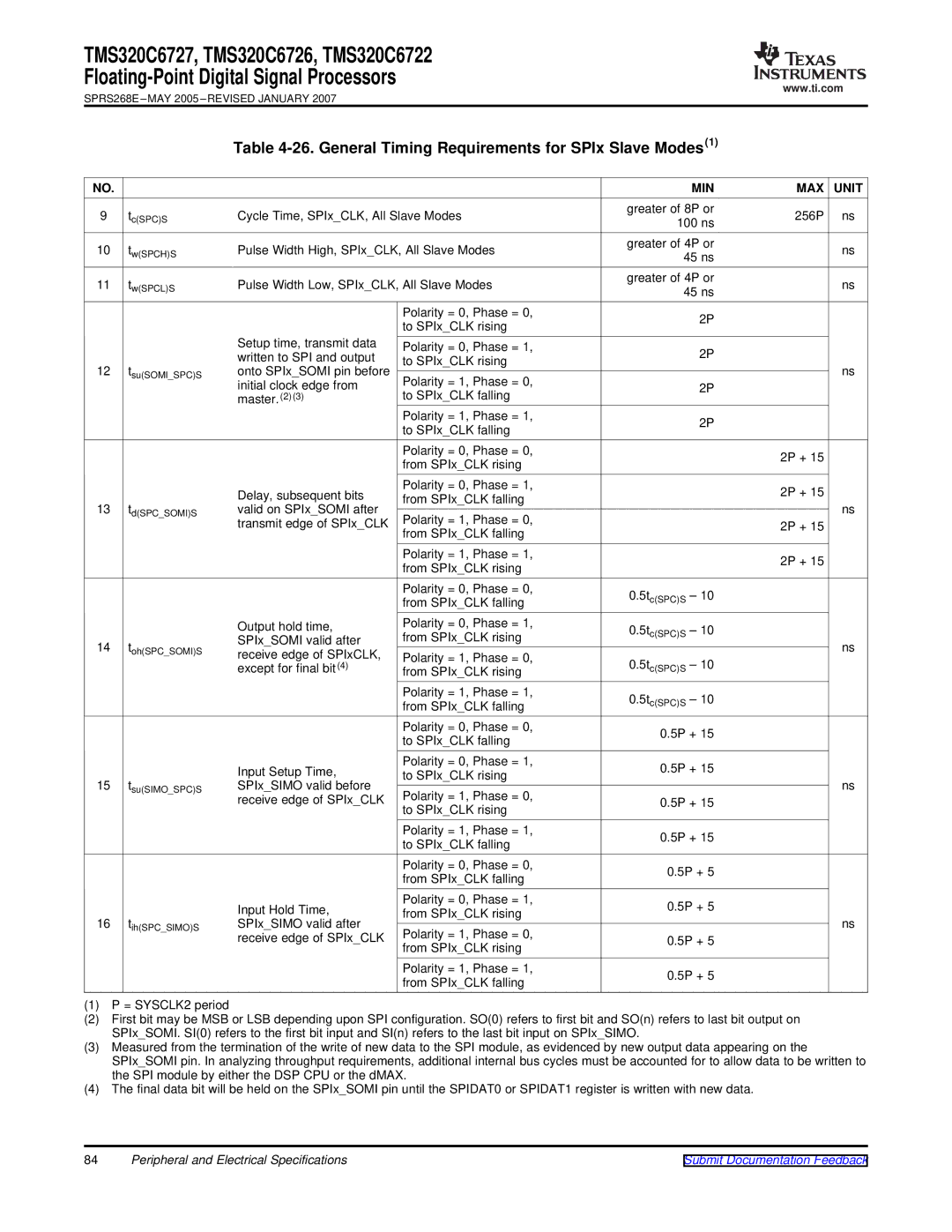
Table 4-26. General Timing Requirements for SPIx Slave Modes(1)
NO.
9tc(SPC)S
10tw(SPCH)S
11tw(SPCL)S
Cycle Time, SPIx_CLK, All Slave Modes
Pulse Width High, SPIx_CLK, All Slave Modes
Pulse Width Low, SPIx_CLK, All Slave Modes
MIN
greater of 8P or 100 ns
greater of 4P or 45 ns
greater of 4P or 45 ns
MAX ![]() UNIT
UNIT ![]()
256P ns
ns
ns
12tsu(SOMI_SPC)S
13td(SPC_SOMI)S
14toh(SPC_SOMI)S
15tsu(SIMO_SPC)S
16tih(SPC_SIMO)S
Setup time, transmit data written to SPI and output onto SPIx_SOMI pin before initial clock edge from master.(2)(3)
Delay, subsequent bits valid on SPIx_SOMI after transmit edge of SPIx_CLK
Output hold time, SPIx_SOMI valid after receive edge of SPIxCLK, except for final bit(4)
Input Setup Time,
SPIx_SIMO valid before receive edge of SPIx_CLK
Input Hold Time, SPIx_SIMO valid after receive edge of SPIx_CLK
Polarity = 0, Phase = 0, to SPIx_CLK rising
Polarity = 0, Phase = 1, to SPIx_CLK rising
Polarity = 1, Phase = 0, to SPIx_CLK falling
Polarity = 1, Phase = 1, to SPIx_CLK falling
Polarity = 0, Phase = 0, from SPIx_CLK rising
Polarity = 0, Phase = 1, from SPIx_CLK falling
Polarity = 1, Phase = 0, from SPIx_CLK falling
Polarity = 1, Phase = 1, from SPIx_CLK rising
Polarity = 0, Phase = 0, from SPIx_CLK falling
Polarity = 0, Phase = 1, from SPIx_CLK rising
Polarity = 1, Phase = 0, from SPIx_CLK rising
Polarity = 1, Phase = 1, from SPIx_CLK falling
Polarity = 0, Phase = 0, to SPIx_CLK falling
Polarity = 0, Phase = 1, to SPIx_CLK rising
Polarity = 1, Phase = 0, to SPIx_CLK rising
Polarity = 1, Phase = 1, to SPIx_CLK falling
Polarity = 0, Phase = 0, from SPIx_CLK falling
Polarity = 0, Phase = 1, from SPIx_CLK rising
Polarity = 1, Phase = 0, from SPIx_CLK rising
Polarity = 1, Phase = 1, from SPIx_CLK falling
2P
2P
2P
2P
0.5tc(SPC)S – 10
0.5tc(SPC)S – 10
0.5tc(SPC)S – 10
0.5tc(SPC)S – 10
0.5P + 15
0.5P + 15
0.5P + 15
0.5P + 15
0.5P + 5
0.5P + 5
0.5P + 5
0.5P + 5
ns
2P + 15
2P + 15
ns
2P + 15
2P + 15
ns
ns
ns
(1)P = SYSCLK2 period
(2)First bit may be MSB or LSB depending upon SPI configuration. SO(0) refers to first bit and SO(n) refers to last bit output on SPIx_SOMI. SI(0) refers to the first bit input and SI(n) refers to the last bit input on SPIx_SIMO.
(3)Measured from the termination of the write of new data to the SPI module, as evidenced by new output data appearing on the
SPIx_SOMI pin. In analyzing throughput requirements, additional internal bus cycles must be accounted for to allow data to be written to the SPI module by either the DSP CPU or the dMAX.
(4)The final data bit will be held on the SPIx_SOMI pin until the SPIDAT0 or SPIDAT1 register is written with new data.
84 | Peripheral and Electrical Specifications | Submit Documentation Feedback |