TMS320C6727, TMS320C6726, TMS320C6722 DSPs
Features
Description
Submit Documentation Feedback
Device Compatibility
Functional Block Diagram
Package Thermal Resistance Characteristics
Contents
Characteristics of the C672x Processors
Device Characteristics
Hardware Features
C6726
CPU Data Paths
Enhanced C67x+ CPU
New Floating-Point Instructions for C67x+ CPU
CPU Interrupt Assignments
CPU Interrupt Assignments
Instruction FLOATING-POINT Improves Operation
Byte Bank
Internal Program/Data ROM and RAM
Program Cache
Cache Mode
Program Cache Control Registers
Register Name Byte Address Description
Block Diagram of Crossbar Switch
High-Performance Crossbar Switch
Label Bridge Description Master Clock Target Clock
Bus Bridges
Csprst
BIT no Name Reset Value Read Write Description
C672x Memory Map
Memory Map Summary
Ffff
Required Boot Pin Settings at Device Reset
Boot Modes
Boot Mode Uhpihcs
SPI0SIMO SPI0CLK
PINCAP7
BIT no Name Description
PINCAP15
Pin Maps
Pin Assignments
Pin Low-Profile Quad Flatpack RFP Suffix-Top View
Terminal Functions
Signal Name RFP GDH
12. Terminal Functions
ZDH
IO/I IPD
Description ZDH
ACLKR0
AHCLKR0/AHCLKR1
AFSR0
AHCLKX0/AHCLKX2
Power Pins 144-Pin RFP Package
Power Pins 256-Terminal GDH/ZDH Package
Development Support
Development
Device Support
Prefix Device Speed Range
TMS 320 C6727 GDH a 250
Device Family
Package Type ‡ §
Documentation Support
C672x devices are documented in the tools v6.0 documentation
Device-Level Configuration Registers
Device Configuration Registers
Options for Configuring SPI0, I2C0, and I2C1
Peripheral Pin Multiplexing Options
Options for Configuring Emif and Uhpi C6727 Only
Options for Configuring SPI1, McASP0, and McASP1 Data Pins
Configuration Option Peripheral
Peripheral Pin Multiplexing Control
PIN First Priority Second Priority Third Priority
Priority of Control of Data Output on Multiplexed Pins
Absolute Maximum Ratings1
Electrical Specifications
Recommended Operating Conditions1
Unit
Dvdd
Parameter Test Conditions MIN TYP MAX Unit
II, IOZ
GDH, CV
Parameter Information Device-Specific Information
Parameter Information
Tester Pin Electronics
Timing Parameter Symbology
Power-Supply Sequencing
Power Supplies
Power-Supply Decoupling
Reset Electrical Data/Timing
Reset
Reset Timing Requirements
MIN MAX Unit
DMAX Device-Specific Information
Dual Data Movement Accelerator dMAX
RAM
DMAX
REQ
REQ RAM
Submit Documentation Feedback
Event Number Event Acronym Event Description
DMAX Peripheral Event Input Assignments
DMAX Peripheral Registers Descriptions
DMAX Configuration Registers
Byte Address Register Name Description
External Interrupts
Emif Device-Specific Information
External Memory Interface Emif
DSP Emif
Reset
Emras
Emwe
Emclk
Emcas
EMWEDQM0
EMWEDQM1
Emif Registers
Emif Peripheral Registers Descriptions
Emif Electrical Data/Timing
Emif Sdram Interface Switching Characteristics
Emif Sdram Interface Timing Requirements
Parameter MIN MAX Unit
Emif Asynchronous Interface Timing Requirements1
Emif Asynchronous Interface Switching Characteristics1
Emras Emcas Emwe
Basic Sdram Write Operation Emclk
Basic Sdram Read Operation
10. Asynchronous Read Select Strobe Mode
Asynchronous Read WE Strobe Mode
12. Asynchronous Write Select Strobe Mode
11. Asynchronous Write WE Strobe Mode
13. Emwait Timing Requirements
Universal Host-Port Interface Uhpi C6727 Only
10. HPI Access Types Selected by UHPIHCNTL10
Uhpi Device-Specific Information
Uhpi Major Modes on C672x
UHPIHD16/HHWIL
DSP
Uhpihasb
Uhpihrw UHPIHDS2G UHPIHDS1G Uhpihcs Uhpihrdy AMUTE2/HINT
External Host MCU AxyC D150 D16 D3117 BE30D
16. Uhpi Multiplexed Host Address/Data Fullword Mode
External Host MCU A172 AxyA D150 D16 D3117 BE30C
17. Uhpi Non-Multiplexed Host Address/Data Fullword Mode
Device-Level Configuration Registers Controlling Uhpi
11. Uhpi Configuration Registers
Uhpi Peripheral Registers Descriptions
Uhpi Internal Registers
Bytead Full Nmux Pagem ENA
BIT no Name Reset Read Description Value Write
318 Reserved
BIT no Name Reset Read Value Write
Hpiamsb Description
Hpiaumb Description
Universal Host-Port Interface Uhpi Read and Write Timing
Uhpi Electrical Data/Timing
15. Uhpi Read and Write Timing Requirements1
16. Uhpi Read and Write Switching Characteristics1
Read Write UHPIHA150
UHPIHDSx
Valid Read data Write data
Uhpihcs Uhpihas UHPIHCNTL10 Uhpihrw Uhpihhwil Hstrobe a
22. Multiplexed Read Timings Using Uhpihas
23. Multiplexed Read Timings With Uhpihas Held High
24. Multiplexed Write Timings With Uhpihas Held High
GIO
Multichannel Audio Serial Ports McASP0, McASP1, and McASP2
DIT Clock Pins Data Pins Comments
17. McASP Configurations on C672x DSP
McASP Peripheral Registers Descriptions
Device-Level Configuration Registers Controlling McASP
Register Byte Description Name Address
McASP Internal Registers
Xevtctl
Xclkchk
DITCSRA0
DITCSRA1
0x4500 020C XBUF3 Transmit buffer register for serializer
313 Reserved
AMUTEIN0
AMUTEIN0 Description
AMUTEIN1 Description
AMUTEIN1
AMUTEIN2
AMUTEIN2
Multichannel Audio Serial Port McASP Timing
McASP Electrical Data/Timing
22. McASP Timing Requirements1
23. McASP Switching Characteristics1
ACLKR/X Clkrp = Clkxp = 0A ACLKR/X Clkrp = Clkxp = 1B
29. McASP Input Timings
ACLKR/X Clkrp = Clkxp = 1A ACLKR/X Clkrp = Clkxp = 0B
30. McASP Output Timings
SPI Device-Specific Information
Serial Peripheral Interface Ports SPI0, SPI1
Master SPI
SPIxSCS SPIxENA SPIxCLK SPIxSOMI SPIxSIMO
Slave SPI
SPI Peripheral Registers Descriptions
24. SPIx Configuration Registers
SPI0 SPI1 Register Name Description Byte Address
Serial Peripheral Interface SPI Timing
SPI Electrical Data/Timing
25. General Timing Requirements for SPIx Master Modes1
26. General Timing Requirements for SPIx Slave Modes1
MIN MAX Unit 2P
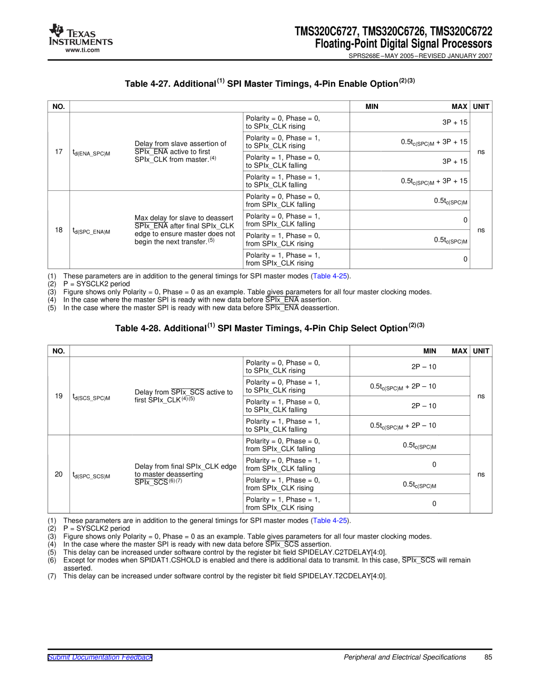
27. Additional1 SPI Master Timings, 4-Pin Enable Option2
29. Additional1 SPI Master Timings, 5-Pin Option2
31. Additional1 SPI Slave Timings, 4-Pin Chip Select Option2
30. Additional1 SPI Slave Timings, 4-Pin Enable Option2
32. Additional1 SPI Slave Timings, 5-Pin Option2
33. SPI Timings-Master Mode
34. SPI Timings-Slave Mode
35. SPI Timings-Master Mode 4-Pin and 5-Pin
36. SPI Timings-Slave Mode 4-Pin and 5-Pin
15.1 I2C Device-Specific Information
Inter-Integrated Circuit Serial Ports I2C0, I2C1
15.2 I2C Peripheral Registers Descriptions
33. I2Cx Configuration Registers
Register Name Description Byte Address
15.3 I2C Electrical Data/Timing
35. I2C Switching Characteristics1
Inter-Integrated Circuit I2C Timing
34. I2C Input Timing Requirements
Parameter
35. I2C Switching Characteristics
I2CxSDA I2CxSCL Stop Start Repeated
16.1 RTI/Digital Watchdog Device-Specific Information
Real-Time Interrupt RTI Timer With Digital Watchdog
Watchdog Key Register Bit Key RTI Interrupt
16.2 RTI/Digital Watchdog Registers Descriptions
Device-Level Configuration Registers Controlling RTI
36. RTI Registers
RTI Internal Registers
Rtidwdctrl
Rtiintflag
Rtidwdprld
Rtiwdstatus
38. Recommended On-Chip Oscillator Components
External Clock Input From Oscillator or Clkin Pin
39. Clkin Timing Requirements
Clock Electrical Data/Timing
PLL Device-Specific Information
Phase-Locked Loop PLL
40. Allowed PLL Operating Conditions
Parameter Default Value Allowed Setting or Range
Board
EMI
41. PLL Controller Registers
PLL Registers Descriptions
ADC, DAC, DSD
CODEC, DIR
Spio
RTI
ADDS/CHANGES/DELETES
Thermal Characteristics for GDH/ZDH Package
Package Thermal Resistance Characteristics
Thermal Characteristics for RFP Package
Standoff Height
Standoff Height
Packaging Information
PowerPAD PCB Footprint
Page
MSL Peak Temp
Orderable Device Status Package Pins Package Eco Plan
Qty
Page
Page
Important Notice

 UNIT
UNIT  2P – 10