Chapter 1: ML605 Evaluation Board
9. PCI Express Endpoint Connectivity
The
The ML605 board trace impedance on all PCIe lanes supports both Gen1 and Gen2 applications. The ML605 supports up to Gen1 x8 and Gen2 x4 as shipped with a
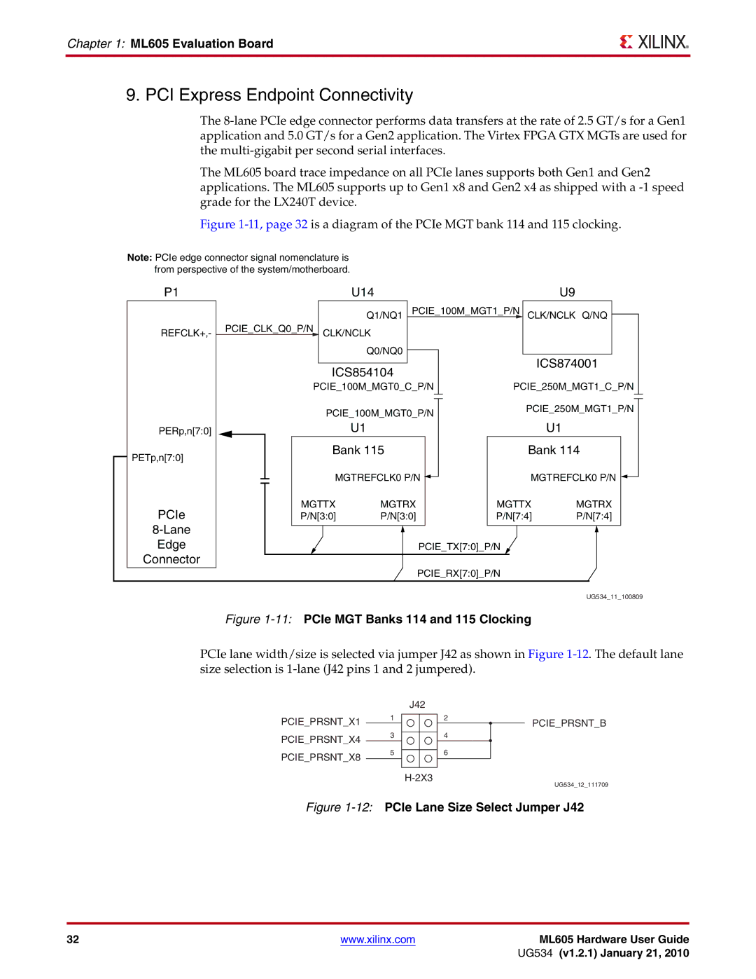
Figure 1-11, page 32 is a diagram of the PCIe MGT bank 114 and 115 clocking.
Note: PCIe edge connector signal nomenclature is |
|
|
| |
from perspective of the system/motherboard. |
|
|
| |
P1 |
| U14 |
| U9 |
|
| Q1/NQ1 PCIE_100M_MGT1_P/N CLK/NCLK Q/NQ | ||
REFCLK+,- | PCIE_CLK_Q0_P/N CLK/NCLK |
|
| |
|
| Q0/NQ0 |
| ICS874001 |
| ICS854104 |
| ||
|
|
| ||
| PCIE_100M_MGT0_C_P/N | PCIE_250M_MGT1_C_P/N | ||
| PCIE_100M_MGT0_P/N | PCIE_250M_MGT1_P/N | ||
|
|
| ||
PERp,n[7:0] |
| U1 |
| U1 |
PETp,n[7:0] | Bank 115 | Bank 114 | ||
|
|
|
| |
| MGTREFCLK0 P/N | MGTREFCLK0 P/N | ||
PCIe | MGTTX | MGTRX | MGTTX | MGTRX |
P/N[3:0] | P/N[3:0] | P/N[7:4] | P/N[7:4] | |
|
|
|
| |
Edge |
| PCIE_TX[7:0]_P/N |
| |
Connector |
|
|
|
|
|
| PCIE_RX[7:0]_P/N |
| |
|
|
|
| UG534_11_100809 |
| Figure |
| ||
PCIe lane width/size is selected via jumper J42 as shown in Figure
|
| J42 |
PCIE_PRSNT_X1 | 1 | 2 |
|
| |
PCIE_PRSNT_X4 | 3 | 4 |
|
|
PCIE_PRSNT_B
PCIE_PRSNT_X8
56
UG534_12_111709
Figure 1-12: PCIe Lane Size Select Jumper J42
32 | www.xilinx.com | ML605 Hardware User Guide |
|
| UG534 (v1.2.1) January 21, 2010 |