Detailed Description
Table 1-3: Voltage Rails (Cont’d)
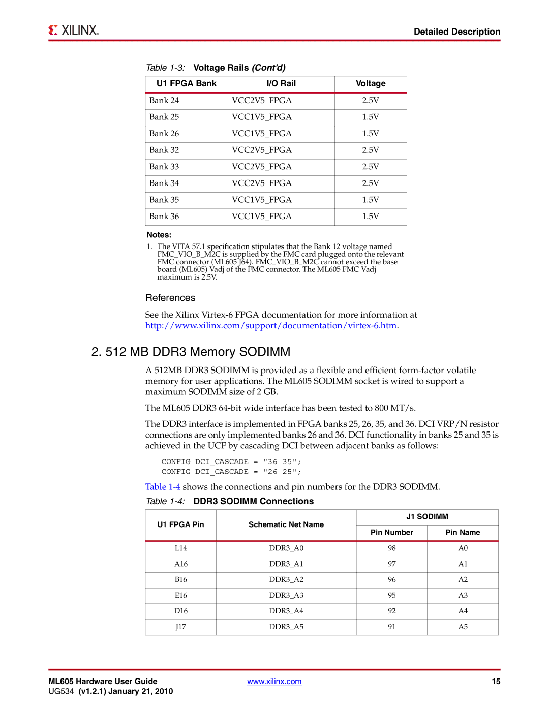
U1 FPGA Bank | I/O Rail | Voltage |
|
|
|
Bank 24 | VCC2V5_FPGA | 2.5V |
|
|
|
Bank 25 | VCC1V5_FPGA | 1.5V |
|
|
|
Bank 26 | VCC1V5_FPGA | 1.5V |
|
|
|
Bank 32 | VCC2V5_FPGA | 2.5V |
|
|
|
Bank 33 | VCC2V5_FPGA | 2.5V |
|
|
|
Bank 34 | VCC2V5_FPGA | 2.5V |
|
|
|
Bank 35 | VCC1V5_FPGA | 1.5V |
|
|
|
Bank 36 | VCC1V5_FPGA | 1.5V |
|
|
|
Notes:
1.The VITA 57.1 specification stipulates that the Bank 12 voltage named FMC_VIO_B_M2C is supplied by the FMC card plugged onto the relevant FMC connector (ML605 J64). FMC_VIO_B_M2C cannot exceed the base board (ML605) Vadj of the FMC connector. The ML605 FMC Vadj maximum is 2.5V.
References
See the Xilinx
2. 512 MB DDR3 Memory SODIMM
A 512MB DDR3 SODIMM is provided as a flexible and efficient
The ML605 DDR3
The DDR3 interface is implemented in FPGA banks 25, 26, 35, and 36. DCI VRP/N resistor connections are only implemented banks 26 and 36. DCI functionality in banks 25 and 35 is achieved in the UCF by cascading DCI between adjacent banks as follows:
CONFIG DCI_CASCADE = "36 35";
CONFIG DCI_CASCADE = "26 25";
Table
Table 1-4: DDR3 SODIMM Connections
U1 FPGA Pin | Schematic Net Name | J1 SODIMM | |
|
| ||
|
| Pin Number | Pin Name |
|
|
|
|
L14 | DDR3_A0 | 98 | A0 |
|
|
|
|
A16 | DDR3_A1 | 97 | A1 |
|
|
|
|
B16 | DDR3_A2 | 96 | A2 |
|
|
|
|
E16 | DDR3_A3 | 95 | A3 |
|
|
|
|
D16 | DDR3_A4 | 92 | A4 |
|
|
|
|
J17 | DDR3_A5 | 91 | A5 |
|
|
|
|
ML605 Hardware User Guide | www.xilinx.com | 15 |
UG534 (v1.2.1) January 21, 2010 |
|
|