Detailed Description
Detailed Description
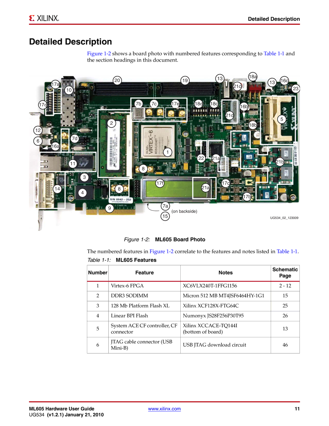
Figure 1-2 shows a board photo with numbered features corresponding to Table 1-1 and the section headings in this document.
17a
10
17d
12
67d
![]() 16a
16a
11
3
14
4
20
2
8
9
|
|
| 19 | 13 | 18a |
|
|
|
| ||
|
|
|
|
| |
|
|
|
|
| 21c |
7b | 7c | 17e |
| 18d 18c | 16b |
|
|
|
|
| |
|
|
|
|
| 21d |
|
|
|
|
| 18b |
1
22 21a
8
17f | 17c |
| 21a |
17b
7a
(on backside)
15
13 16c
23
5
21b
UG534_02_123009
Figure 1-2: ML605 Board Photo
The numbered features in Figure
Table | ML605 Features |
|
| |
|
|
|
|
|
Number |
| Feature | Notes | Schematic |
| Page | |||
|
|
|
| |
|
|
|
|
|
1 |
| 2 - 12 | ||
|
|
|
|
|
2 |
| DDR3 SODIMM | Micron 512 MB | 15 |
|
|
|
|
|
3 |
| 128 Mb Platform Flash XL | Xilinx | 25 |
|
|
|
|
|
4 |
| Linear BPI Flash | Numonyx JS28F256P30T95 | 26 |
|
|
|
|
|
5 |
| System ACE CF controller, CF | Xilinx | 13 |
| connector | (bottom of board) | ||
|
|
| ||
|
|
|
|
|
6 |
| JTAG cable connector (USB | USB JTAG download circuit | 46 |
| ||||
|
|
|
| |
|
|
|
|
|
ML605 Hardware User Guide | www.xilinx.com | 11 |
UG534 (v1.2.1) January 21, 2010 |
|
|
