Chapter 1: ML605 Evaluation Board
Block Diagram
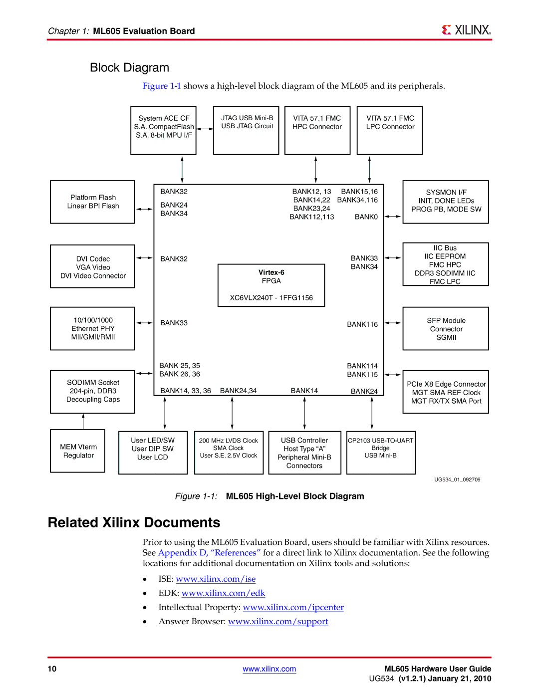
Figure 1-1 shows a high-level block diagram of the ML605 and its peripherals.
System ACE CF |
|
|
| JTAG USB |
S.A. CompactFlash |
|
|
| USB JTAG Circuit |
S.A. |
|
|
|
|
|
|
|
|
|
VITA 57.1 FMC HPC Connector
VITA 57.1 FMC LPC Connector
Platform Flash
Linear BPI Flash
DVI Codec
VGA Video
DVI Video Connector
10/100/1000 Ethernet PHY MII/GMII/RMII
SODIMM Socket
Decoupling Caps
BANK32 | BANK12, 13 | BANK15,16 | |
BANK24 | BANK14,22 | BANK34,116 | |
BANK23,24 |
| ||
BANK34 |
| ||
BANK112,113 | BANK0 | ||
|
BANK32 |
| BANK33 |
|
| BANK34 |
| ||
|
| |
| FPGA |
|
| XC6VLX240T - 1FFG1156 |
|
BANK33 |
| BANK116 |
|
BANK 25, 35 |
| BANK114 |
BANK 26, 36 |
| BANK115 |
BANK14, 33, 36 BANK24,34 | BANK14 | BANK24 |
SYSMON I/F
INIT, DONE LEDs
PROG PB, MODE SW
IIC Bus
IIC EEPROM
FMC HPC
DDR3 SODIMM IIC
FMC LPC
SFP Module
Connector
SGMII
PCIe X8 Edge Connector
MGT SMA REF Clock
MGT RX/TX SMA Port
MEM Vterm
Regulator
User LED/SW
User DIP SW
User LCD
200 MHz LVDS Clock
SMA Clock
User S.E. 2.5V Clock
USB Controller
Host Type “A”
Peripheral
Connectors
CP2103
Bridge
USB
UG534_01_092709
Figure 1-1: ML605 High-Level Block Diagram
Related Xilinx Documents
Prior to using the ML605 Evaluation Board, users should be familiar with Xilinx resources. See Appendix D, “References” for a direct link to Xilinx documentation. See the following locations for additional documentation on Xilinx tools and solutions:
•ISE: www.xilinx.com/ise
•EDK: www.xilinx.com/edk
•Intellectual Property: www.xilinx.com/ipcenter
•Answer Browser: www.xilinx.com/support
10 | www.xilinx.com | ML605 Hardware User Guide |
|
| UG534 (v1.2.1) January 21, 2010 |