Chapter 1: ML605 Evaluation Board
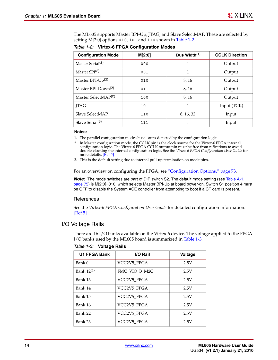
The ML605 supports Master
Table 1-2: Virtex-6 FPGA Configuration Modes
Configuration Mode | M[2:0] | Bus Width(1) | CCLK Direction |
Master Serial(2) | 000 | 1 | Output |
Master SPI(2) | 001 | 1 | Output |
Master | 010 | 8, 16 | Output |
Master | 011 | 8, 16 | Output |
Master SelectMAP(2) | 100 | 8, 16 | Output |
JTAG | 101 | 1 | Input (TCK) |
|
|
|
|
Slave SelectMAP | 110 | 8, 16, 32 | Input |
|
|
|
|
Slave Serial(3) | 111 | 1 | Input |
Notes:
1.The parallel configuration modes bus is
2.In Master configuration mode, the CCLK pin is the clock source for the
3.This is the default setting due to internal
For an overview on configuring the FPGA, see “Configuration Options,” page 73.
Note: The mode switches are part of DIP switch S2. The default mode setting (see Table
References
See the
I/O Voltage Rails
There are 16 I/O banks available on the
Table 1-3: Voltage Rails
| U1 FPGA Bank | I/O Rail | Voltage |
|
|
|
|
|
|
| Bank 0 | VCC2V5_FPGA | 2.5V |
|
|
|
|
|
|
| Bank 12(1) | FMC_VIO_B_M2C | 2.5V |
|
| Bank 13 | VCC2V5_FPGA | 2.5V |
|
|
|
|
|
|
| Bank 14 | VCC2V5_FPGA | 2.5V |
|
|
|
|
|
|
| Bank 15 | VCC2V5_FPGA | 2.5V |
|
|
|
|
|
|
| Bank 16 | VCC2V5_FPGA | 2.5V |
|
|
|
|
|
|
| Bank 22 | VCC2V5_FPGA | 2.5V |
|
|
|
|
|
|
| Bank 23 | VCC2V5_FPGA | 2.5V |
|
|
|
|
|
|
|
|
|
|
|
14 |
| www.xilinx.com | ML605 Hardware User Guide | |
|
|
| UG534 (v1.2.1) January 21, 2010 | |
