Detailed Description
ML605 Flash Boot Options
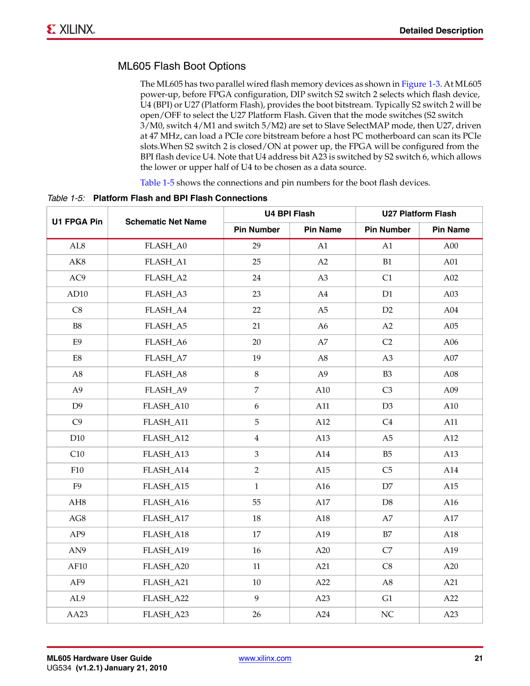
The ML605 has two parallel wired flash memory devices as shown in Figure
Table
Table
U1 FPGA Pin | Schematic Net Name | U4 BPI Flash | U27 Platform Flash | |||
|
|
|
| |||
Pin Number | Pin Name | Pin Number | Pin Name | |||
|
| |||||
|
|
|
|
|
| |
AL8 | FLASH_A0 | 29 | A1 | A1 | A00 | |
|
|
|
|
|
| |
AK8 | FLASH_A1 | 25 | A2 | B1 | A01 | |
|
|
|
|
|
| |
AC9 | FLASH_A2 | 24 | A3 | C1 | A02 | |
|
|
|
|
|
| |
AD10 | FLASH_A3 | 23 | A4 | D1 | A03 | |
|
|
|
|
|
| |
C8 | FLASH_A4 | 22 | A5 | D2 | A04 | |
|
|
|
|
|
| |
B8 | FLASH_A5 | 21 | A6 | A2 | A05 | |
|
|
|
|
|
| |
E9 | FLASH_A6 | 20 | A7 | C2 | A06 | |
|
|
|
|
|
| |
E8 | FLASH_A7 | 19 | A8 | A3 | A07 | |
|
|
|
|
|
| |
A8 | FLASH_A8 | 8 | A9 | B3 | A08 | |
|
|
|
|
|
| |
A9 | FLASH_A9 | 7 | A10 | C3 | A09 | |
|
|
|
|
|
| |
D9 | FLASH_A10 | 6 | A11 | D3 | A10 | |
|
|
|
|
|
| |
C9 | FLASH_A11 | 5 | A12 | C4 | A11 | |
|
|
|
|
|
| |
D10 | FLASH_A12 | 4 | A13 | A5 | A12 | |
|
|
|
|
|
| |
C10 | FLASH_A13 | 3 | A14 | B5 | A13 | |
|
|
|
|
|
| |
F10 | FLASH_A14 | 2 | A15 | C5 | A14 | |
|
|
|
|
|
| |
F9 | FLASH_A15 | 1 | A16 | D7 | A15 | |
|
|
|
|
|
| |
AH8 | FLASH_A16 | 55 | A17 | D8 | A16 | |
|
|
|
|
|
| |
AG8 | FLASH_A17 | 18 | A18 | A7 | A17 | |
|
|
|
|
|
| |
AP9 | FLASH_A18 | 17 | A19 | B7 | A18 | |
|
|
|
|
|
| |
AN9 | FLASH_A19 | 16 | A20 | C7 | A19 | |
|
|
|
|
|
| |
AF10 | FLASH_A20 | 11 | A21 | C8 | A20 | |
|
|
|
|
|
| |
AF9 | FLASH_A21 | 10 | A22 | A8 | A21 | |
|
|
|
|
|
| |
AL9 | FLASH_A22 | 9 | A23 | G1 | A22 | |
|
|
|
|
|
| |
AA23 | FLASH_A23 | 26 | A24 | NC | A23 | |
|
|
|
|
|
| |
ML605 Hardware User Guide | www.xilinx.com | 21 |
UG534 (v1.2.1) January 21, 2010 |
|
|