Detailed Description
Table
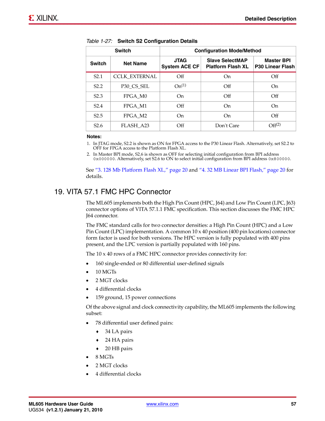
| Switch |
| Configuration Mode/Method | |||
|
|
|
|
|
| |
Switch | Net Name | JTAG |
| Slave SelectMAP | Master BPI | |
System ACE CF | Platform Flash XL | P30 Linear Flash | ||||
|
| |||||
|
|
|
|
|
| |
S2.1 | CCLK_EXTERNAL | Off |
| On | Off | |
|
|
|
|
|
| |
S2.2 | P30_CS_SEL | On(1) |
| Off | On | |
S2.3 | FPGA_M0 | On |
| Off | Off | |
|
|
|
|
|
| |
S2.4 | FPGA_M1 | Off |
| On | On | |
|
|
|
|
|
| |
S2.5 | FPGA_M2 | On |
| On | Off | |
|
|
|
|
|
| |
S2.6 | FLASH_A23 | Off |
| Don't Care | Off(2) | |
Notes:
1.In JTAG mode, S2.2 is shown as ON for FPGA access to the P30 Linear Flash. Alternatively, set S2.2 to OFF for FPGA access to the Platform Flash XL.
2.In Master BPI mode, S2.6 is shown as OFF for selecting initial configuration from BPI address 0x000000. Alternatively, set S2.6 to ON to select initial configuration from BPI address 0x800000.
See “3. 128 Mb Platform Flash XL,” page 20 and “4. 32 MB Linear BPI Flash,” page 20 for details.
19. VITA 57.1 FMC HPC Connector
The ML605 implements both the High Pin Count (HPC, J64) and Low Pin Count (LPC, J63) connector options of VITA 57.1.1 FMC specification. This section discusses the FMC HPC J64 connector.
The FMC standard calls for two connector densities: a High Pin Count (HPC) and a Low Pin Count (LPC) implementation. A common 10 x 40 position (400 pin locations) connector form factor is used for both versions. The HPC version is fully populated with 400 pins present, and the LPC version is partially populated with 160 pins.
The 10 x 40 rows of a FMC HPC connector provides connectivity for:
•160
•10 MGTs
•2 MGT clocks
•4 differential clocks
•159 ground, 15 power connections
Of the above signal and clock connectivity capability, the ML605 implements the following subset:
•78 differential user defined pairs:
♦34 LA pairs
♦24 HA pairs
♦20 HB pairs
•8 MGTs
•2 MGT clocks
•4 differential clocks
ML605 Hardware User Guide | www.xilinx.com | 57 |
UG534 (v1.2.1) January 21, 2010 |
|
|