|
|
|
|
|
|
| PLB PCI Full Bridge (v1.00a) |
|
|
|
|
|
|
|
|
|
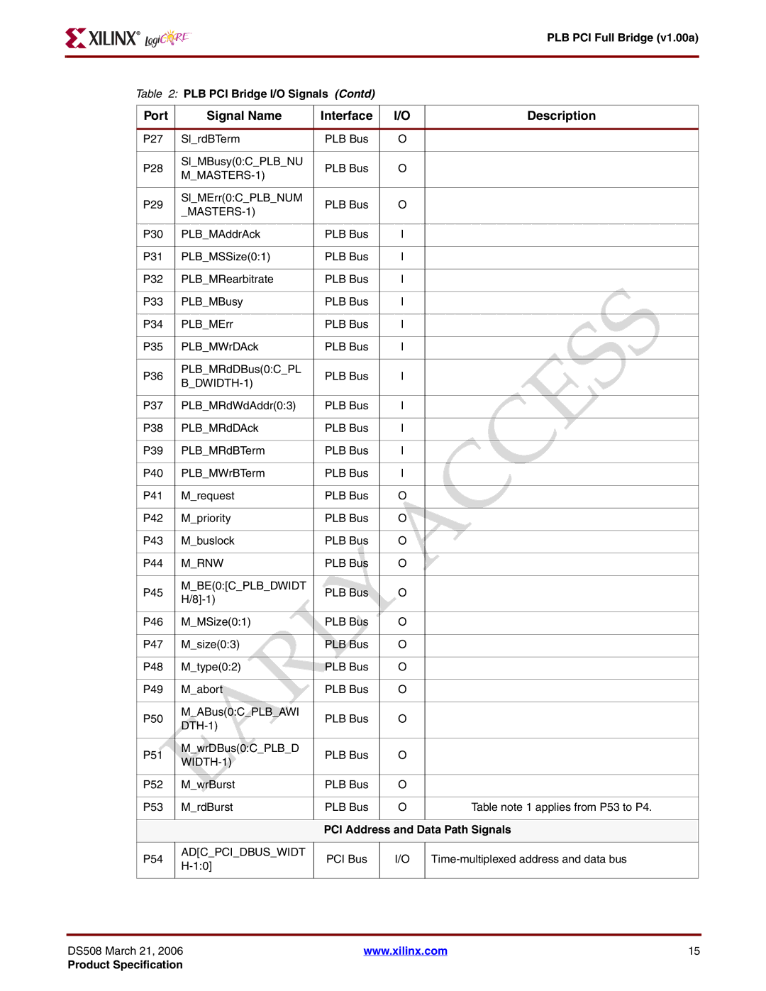
| Table 2: PLB PCI Bridge I/O Signals (Contd) |
|
| |||
|
|
|
|
|
|
|
|
|
|
| Port | Signal Name | Interface | I/O | Description |
|
|
|
|
|
|
|
|
|
|
| P27 | Sl_rdBTerm | PLB Bus | O |
|
|
|
|
|
|
|
|
|
|
|
| P28 | Sl_MBusy(0:C_PLB_NU | PLB Bus | O |
|
|
|
|
| ||||
|
|
|
|
|
|
| |
|
|
|
|
|
|
|
|
|
|
| P29 | Sl_MErr(0:C_PLB_NUM | PLB Bus | O |
|
|
|
|
|
| |||
|
|
|
|
|
|
| |
|
|
|
|
|
|
|
|
|
|
| P30 | PLB_MAddrAck | PLB Bus | I |
|
|
|
|
|
|
|
|
|
|
|
| P31 | PLB_MSSize(0:1) | PLB Bus | I |
|
|
|
|
|
|
|
|
|
|
|
| P32 | PLB_MRearbitrate | PLB Bus | I |
|
|
|
|
|
|
|
|
|
|
|
| P33 | PLB_MBusy | PLB Bus | I |
|
|
|
|
|
|
|
|
|
|
|
| P34 | PLB_MErr | PLB Bus | I |
|
|
|
|
|
|
|
|
|
|
|
| P35 | PLB_MWrDAck | PLB Bus | I |
|
|
|
|
|
|
|
|
|
|
|
| P36 | PLB_MRdDBus(0:C_PL | PLB Bus | I |
|
|
|
|
|
| |||
|
|
|
|
|
|
| |
|
|
|
|
|
|
|
|
|
|
| P37 | PLB_MRdWdAddr(0:3) | PLB Bus | I |
|
|
|
|
|
|
|
|
|
|
|
| P38 | PLB_MRdDAck | PLB Bus | I |
|
|
|
|
|
|
|
|
|
|
|
| P39 | PLB_MRdBTerm | PLB Bus | I |
|
|
|
|
|
|
|
|
|
|
|
| P40 | PLB_MWrBTerm | PLB Bus | I |
|
|
|
|
|
|
|
|
|
|
|
| P41 | M_request | PLB Bus | O |
|
|
|
|
|
|
|
|
|
|
|
| P42 | M_priority | PLB Bus | O |
|
|
|
|
|
|
|
|
|
|
|
| P43 | M_buslock | PLB Bus | O |
|
|
|
|
|
|
|
|
|
|
|
| P44 | M_RNW | PLB Bus | O |
|
|
|
|
|
|
|
|
|
|
|
| P45 | M_BE(0:[C_PLB_DWIDT | PLB Bus | O |
|
|
|
|
| ||||
|
|
|
|
|
|
| |
|
|
|
|
|
|
|
|
|
|
| P46 | M_MSize(0:1) | PLB Bus | O |
|
|
|
|
|
|
|
|
|
|
|
| P47 | M_size(0:3) | PLB Bus | O |
|
|
|
|
|
|
|
|
|
|
|
| P48 | M_type(0:2) | PLB Bus | O |
|
|
|
|
|
|
|
|
|
|
|
| P49 | M_abort | PLB Bus | O |
|
|
|
|
|
|
|
|
|
|
|
| P50 | M_ABus(0:C PLB AWI | PLB Bus | O |
|
|
|
|
| ||||
|
|
|
|
|
|
| |
|
|
|
|
|
|
|
|
|
|
| P51 | M wrDBus(0:C PLB D | PLB Bus | O |
|
|
|
|
| ||||
|
|
|
|
|
|
| |
|
|
|
|
|
|
|
|
|
|
| P52 | M wrBurst | PLB Bus | O |
|
|
|
|
|
|
|
|
|
|
|
| P53 | M rdBurst | PLB Bus | O | Table note 1 applies from P53 to P4. |
|
|
|
|
|
|
|
|
|
|
|
|
| PCI Address and Data Path Signals | ||
|
|
|
|
|
|
|
|
|
|
| P54 | AD[C_PCI_DBUS_WIDT | PCI Bus | I/O | |
|
|
| |||||
|
|
|
|
|
|
| |
|
|
|
|
|
|
|
|
DS508 March 21, 2006 | www.xilinx.com | 15 |
Product Specification
