PLB PCI Full Bridge (v1.00a)
Configuration Address Port Register Description
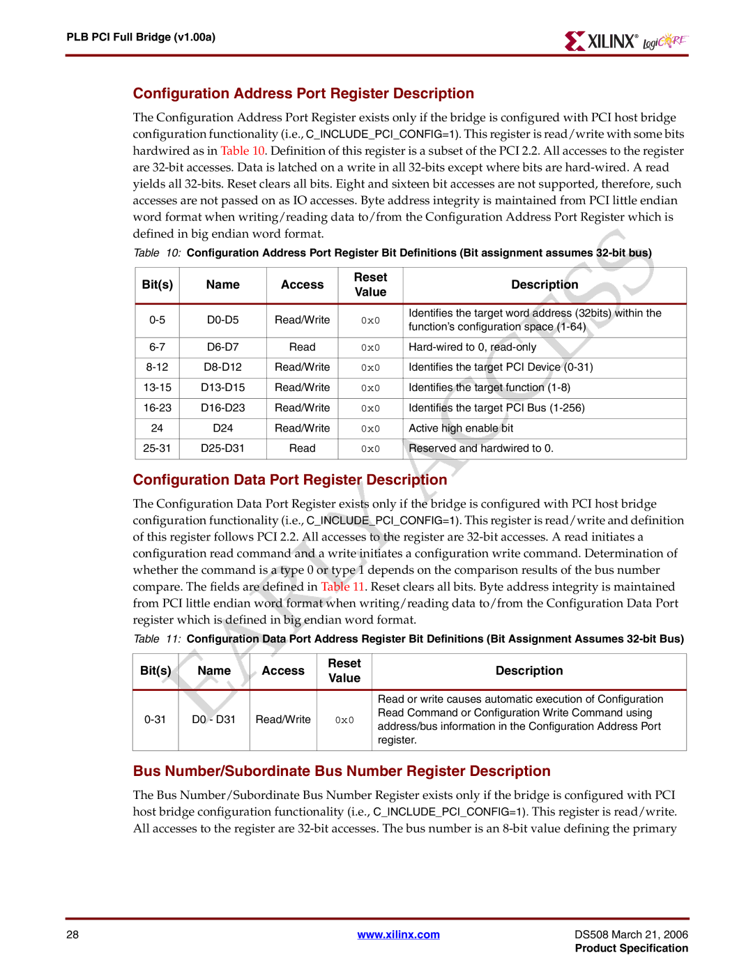
The Configuration Address Port Register exists only if the bridge is configured with PCI host bridge configuration functionality (i.e., C_INCLUDE_PCI_CONFIG=1). This register is read/write with some bits hardwired as in Table 10. Definition of this register is a subset of the PCI 2.2. All accesses to the register are
Table 10: Configuration Address Port Register Bit Definitions (Bit assignment assumes
Bit(s) | Name | Access | Reset | Description | |
Value | |||||
|
|
|
| ||
|
|
|
|
| |
Read/Write | 0x0 | Identifies the target word address (32bits) within the | |||
function’s configuration space | |||||
|
|
|
| ||
|
|
|
|
| |
Read | 0x0 | ||||
|
|
|
|
| |
Read/Write | 0x0 | Identifies the target PCI Device | |||
|
|
|
|
| |
Read/Write | 0x0 | Identifies the target function | |||
|
|
|
|
| |
Read/Write | 0x0 | Identifies the target PCI Bus | |||
|
|
|
|
| |
24 | D24 | Read/Write | 0x0 | Active high enable bit | |
|
|
|
|
| |
Read | 0x0 | Reserved and hardwired to 0. | |||
|
|
|
|
|
Configuration Data Port Register Description
The Configuration Data Port Register exists only if the bridge is configured with PCI host bridge configuration functionality (i.e., C INCLUDE PCI_CONFIG=1). This register is read/write and definition of this register follows PCI 2.2. All accesses to the register are
Table 11: Configuration Data Port Address Register Bit Definitions (Bit Assignment Assumes
Bit(s) | Name | Access | Reset | Description | |
Value | |||||
|
|
|
| ||
|
|
|
|
| |
|
|
|
| Read or write causes automatic execution of Configuration | |
D0 - D31 | Read/Write | 0x0 | Read Command or Configuration Write Command using | ||
address/bus information in the Configuration Address Port | |||||
|
|
|
| ||
|
|
|
| register. | |
|
|
|
|
|
Bus Number/Subordinate Bus Number Register Description
The Bus Number/Subordinate Bus Number Register exists only if the bridge is configured with PCI host bridge configuration functionality (i.e., C_INCLUDE_PCI_CONFIG=1). This register is read/write. All accesses to the register are
28 | www.xilinx.com | DS508 March 21, 2006 |
|
| Product Specification |