PLB PCI Full Bridge (v1.00a)
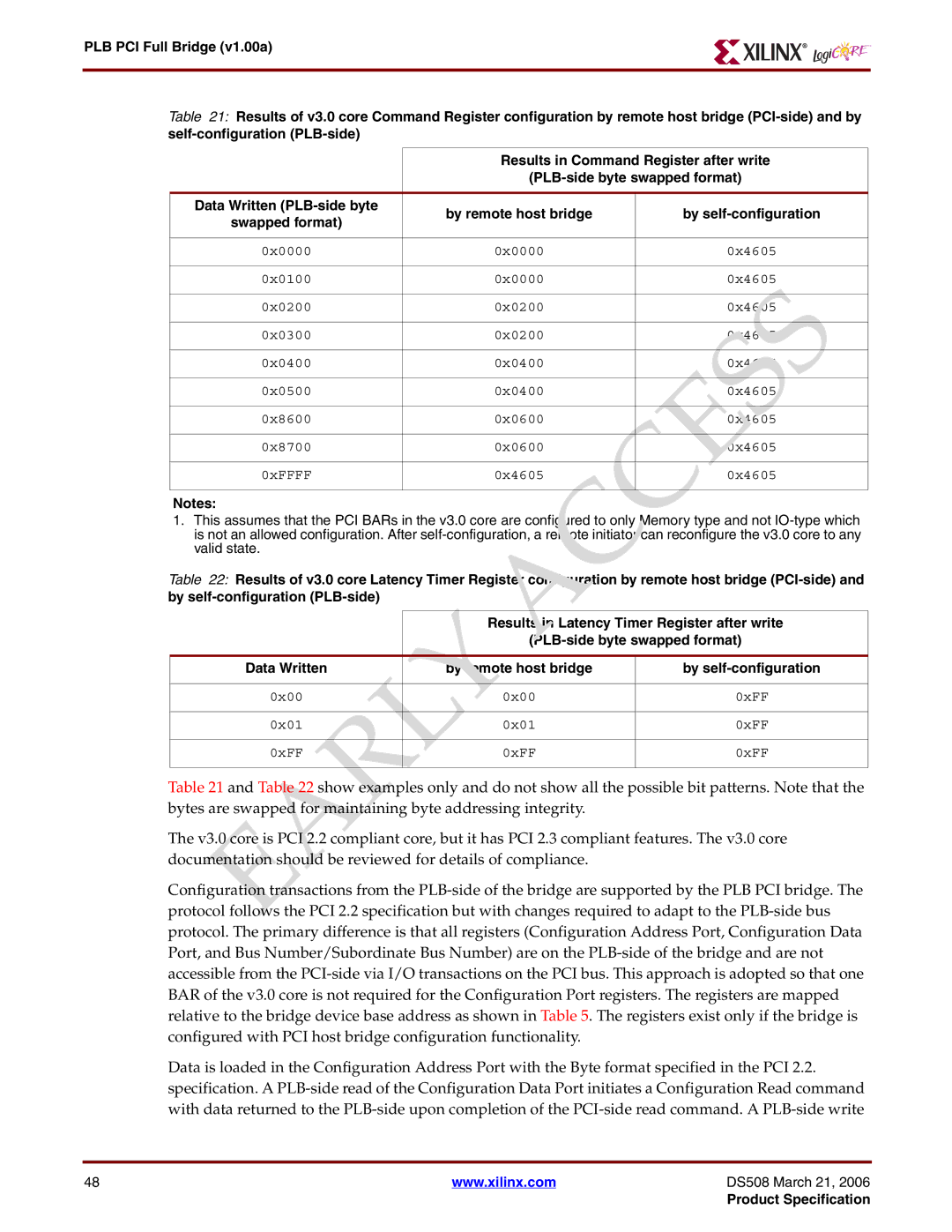
Table 21: Results of v3.0 core Command Register configuration by remote host bridge
| Results in Command Register after write | ||
| |||
|
|
| |
Data Written | by remote host bridge | by | |
swapped format) | |||
|
| ||
|
|
| |
0x0000 | 0x0000 | 0x4605 | |
|
|
| |
0x0100 | 0x0000 | 0x4605 | |
|
|
| |
0x0200 | 0x0200 | 0x4605 | |
|
|
| |
0x0300 | 0x0200 | 0x4605 | |
|
|
| |
0x0400 | 0x0400 | 0x4605 | |
|
|
| |
0x0500 | 0x0400 | 0x4605 | |
|
|
| |
0x8600 | 0x0600 | 0x4605 | |
|
|
| |
0x8700 | 0x0600 | 0x4605 | |
|
|
| |
0xFFFF | 0x4605 | 0x4605 | |
|
|
| |
Notes:
1.This assumes that the PCI BARs in the v3.0 core are configured to only Memory type and not
Table 22: Results of v3.0 core Latency Timer Register configuration by remote host bridge
| Results in Latency Timer Register after write | |
| ||
|
|
|
Data Written | by remote host bridge | by |
|
|
|
0x00 | 0x00 | 0xFF |
|
|
|
0x01 | 0x01 | 0xFF |
|
|
|
0xFF | 0xFF | 0xFF |
|
|
|
Table 21 and Table 22 show examples only and do not show all the possible bit patterns. Note that the bytes are swapped for maintaining byte addressing integrity.
The v3.0 core is PCI 2.2 compliant core, but it has PCI 2.3 compliant features. The v3.0 core documentation should be reviewed for details of compliance.
Configuration transactions from the
Data is loaded in the Configuration Address Port with the Byte format specified in the PCI 2.2. specification. A
48 | www.xilinx.com | DS508 March 21, 2006 |
|
| Product Specification |