Data Manual
Important Notice
Contents
−10
PC Card Controller Programming Model −1
ExCA Compatibility Registers Functions 0 and 1 −1
Ohci Registers −1
Ohci Controller Programming Model −1
Vii
TI Extension Registers −1
PHY Register Configuration 10−1
Viii
SD Host Controller Programming Model −1
Flash Media Controller Programming Model −1
Smart Card Controller Programming Model −1
Mechanical Information 15−1
Electrical Characteristics −1
Xii
List of Illustrations
Xiii
List of Tables
Xiv
Functions 0 and 1 PCI Configuration Register Map
Title −13
Xvi
Xvii
Xviii
1 PCI7621 Controller
Controller Functional Description
3 PCI7611 Controller
2 PCI7421 Controller
Multifunctional Terminals
PCI Bus Power Management
Power Switch Interface
4 PCI7411 Controller
PCI Bus Interface Specification for PCI-to-CardBus Bridges
Features
Related Documents
PCI Local Bus Specification Revision
Trademarks
Term Definitions
Terms and Definitions
Ordering Information
−1. Terms and Definitions
Page
Terminal Descriptions
−2. PCI7421 GHK/ZHK-Package Terminal Diagram
−3. PCI7611 GHK/ZHK-Package Terminal Diagram
−4. PCI7411 GHK/ZHK-Package Terminal Diagram
Terminal Signal Name Number
−1. Signal Names by GHK Terminal Number
VCC Acperr
Breset
ACC/BE2
VCC
Latch
Scclk
BCC/BE0 BCE1
SCVCC5V
Vsspll
Grst Frame
GNT Perr
RIOUT/PME
Signal Name Terminal Number
−2. CardBus PC Card Signal Names Sorted Alphabetically
Prst GND
Sdcmd
PC2TEST3
Perr Trdy GND
Signal Terminal Signal Name Number
−3 -Bit PC Card Signal Names Sorted Alphabetically
−12
−13
Detailed Terminal Descriptions
−14
−4. Power Supply Terminals
−6. PCI System Terminals
−5. PC Card Power Switch Terminals
−15
−16
−7. PCI Address and Data Terminals
−17
−8. PCI Interface Control Terminals
−18
−9. Multifunction and Miscellaneous Terminals
−10 -Bit PC Card Address and Data Terminals
Stschg
−11 -Bit PC Card Interface Control Terminals
AOE
PCIO3 Vccb
−12. CardBus PC Card Interface System Terminals
BCAD0
−13. CardBus PC Card Address and Data Terminals
BCCD2
−14. CardBus PC Card Interface Control Terminals
Cstop
−26
−15. Ieee 1394 Physical Layer Terminals
−17. Memory Stick/PRO Terminals
−16. SD/MMC Terminals
−27
−28
−18. Smart Media/XD Terminals
−19. Smart Card Terminals †
−30
SD/MMC
Power Supply Sequencing
Eeprom
SD/MMC MS/MSPRO
1 1394 PCI Bus Master
I/O Characteristics
Clamping Voltages
Peripheral Component Interconnect PCI Interface
Serial Eeprom I2C Bus
Device Resets
VCC Grst Prst Pclk
ROM A1 SCL A2 SDA VCC
Functions 0 and 1 CardBus Subsystem Identification
Function 4 SD Host Subsystem Identification
PC Card Applications
Function 2 Ohci 1394 Subsystem Identification
Function 3 Flash Media Subsystem Identification
Low Voltage CardBus Card Detection
PC Card Insertion/Removal and Recognition
UltraMedia Card Detection
VCC VPP/VCORE
Flash Media Card Detection
−2. PC Card-Card Detect and Voltage Sense Connections
CD2//CCD2 CD1//CCD1 VS2//CVS2 VS1//CVS1
−5. TPS2226 Control Logic-xVPP
Internal Ring Oscillator
−3. TPS2228 Control Logic-xVPP/VCORE
−4. TPS2228 Control Logic-xVCC
Spkrout Binaryspkr
LED Socket Activity Indicators
Integrated Pullup Resistors for PC Card Interface
Spkrout and Caudpwm Usage
LED
CardBus Socket Registers
11 48-MHz Clock Requirements
−7. CardBus Socket Registers
Serial-Bus Interface Protocol
Accessing Serial-Bus Devices Through Software
Serial Eeprom Interface
Serial-Bus Interface Implementation
−8. Serial-Bus Protocol Acknowledge
−7. Serial-Bus Start/Stop Conditions and Bit Transfers
−10. Serial-Bus Protocol-Byte Read
Serial-Bus Eeprom Application
Serial ROM Byte Description Offset
−9. Eeprom Loading Map
GPE
PCI 2Eh, subsystem ID, byte
LinkEnh HCControl.Program Phy Enable
PCI 2Ch, subsystem vendor ID, byte
PCI 2Dh, subsystem vendor ID, byte
Programmable Interrupt Subsystem
−10. Interrupt Mask and Flag Registers
PC Card Functional and Card Status Change Interrupts
Card Type Event Mask Flag
Interrupt Masks and Flags
Card Type Event Signal Description
−11. PC Card Interrupt Events and Description
Using Parallel PCI Interrupts
Using Parallel IRQ Interrupts
−12. Interrupt Pin Register Cross Reference
Power Management Overview
Using Serialized Irqser Interrupts
SMI Support in the PCI7x21/PCI7x11 Controller
1 1394 Power Management Function
Supply VCC Vren Vrport
CardBus PC Card Power Management
Integrated Low-Dropout Voltage Regulator LDO-VR
CardBus Functions 0 and 1 Clock Run Protocol
Reset GNT Suspend Pclk
5 16-Bit PC Card Power Management
Suspend Mode
Requirements for Suspend Mode
Cstsmask CSC Ringen RI Cdresume
Ring Indicate
Rienb Riout
−15. Power-Management Registers
PCI Power Management
Power-management control/status CSR
−18. Function 4 Power-Management Registers
CardBus Bridge Power Management
−16. Function 2 Power-Management Registers
−17. Function 3 Power-Management Registers
Acpi Support
Master List of PME Context Bits and Global Reset-Only Bits
−28
−29
PHY Port Cable Connection
Ieee 1394 Application Information
−31
Crystal Selection
Cphy + CBD
Bus Reset
−32
−33
−34
Access TAG Name Meaning
PCI Configuration Register Map Functions 0
−1. Bit Field Access Tag Descriptions
−2. Functions 0 and 1 PCI Configuration Register Map
Vendor ID
Vendor ID Register
Device ID Register Functions 0
Device ID-Smart Card enabled
Device ID
BIT Signal Type Function
Command Register
Command
−3. Command Register Description
Status
Status Register
−4. Status Register Description
Class Code Register
Revision ID Register
Cache Line Size Register
Bist Register
Latency Timer Register
Register Latency timer
Header Type Register
Register Capability pointer
CardBus Socket Registers/ExCA Base Address Register
Capability Pointer Register
CardBus socket registers/ExCA base address
Secondary status
Secondary Status Register
−5. Secondary Status Register Description
CardBus Bus Number Register
PCI Bus Number Register
Subordinate Bus Number Register
Memory base registers 0
CardBus Latency Timer Register
Register CardBus latency timer
CardBus Memory Base Registers 0
Base registers 0
CardBus Memory Limit Registers 0
CardBus I/O Base Registers 0
Memory limit registers 0
Register Interrupt line
CardBus I/O Limit Registers 0
Interrupt Line Register
Limit registers 0
Interrupt pin − PCI function
Interrupt Pin Register
Bridge control
Bridge Control Register
Interrupt pin
−6. Interrupt Pin Register Cross Reference
Subsystem vendor ID
Subsystem Vendor ID Register
PC Card 16-bit I/F legacy-mode base-address
Subsystem ID Register
PC Card 16-Bit I/F Legacy-Mode Base-Address Register
Subsystem ID
System control
System Control Register
−8. System Control Register Description
−8 . System Control Register Description
Register Mccd debounce
Mccd Debounce Register
General control
General Control Register
General control
−9. General Control Register Description
General-purpose event status
General-Purpose Event Status Register
−10. General-Purpose Event Status Register Description
General-Purpose Input Register
General-Purpose Event Enable Register
General-purpose output
General-Purpose Output Register
−13. General-Purpose Output Register Description
Multifunction routing status
Multifunction Routing Status Register
−14. Multifunction Routing Status Register Description
Retry status
Retry Status Register
−15. Retry Status Register Description
Card control
Card Control Register
−16. Card Control Register Description
Device control
Device Control Register
−17. Device Control Register Description
Diagnostic
Diagnostic Register
−18. Diagnostic Register Description
Register Next item pointer
Capability ID Register
Next Item Pointer Register
Register Capability ID
Power management capabilities
Power Management Capabilities Register
−19. Power Management Capabilities Register Description
Power management control/status
Power Management Control/Status Register
−20. Power Management Control/Status Register Description
Bpccen
Power-Management Data Register
Power management control/status bridge support extensions
Power-management data
−22. Serial Bus Data Register Description
Serial Bus Data Register
Serial Bus Index Register
Serial bus data
Rwcmd
Serial Bus Slave Address Register
Register Serial bus slave address
−24. Serial Bus Slave Address Register Description
Serial bus control/status
Serial Bus Control/Status Register
−25. Serial Bus Control/Status Register Description
−38
ExCA Compatibility Registers Functions 0
−1. ExCA Register Access Through I/O
−1. ExCA Registers and Offsets
Exca Register Name PCI Memory Address Exca Offset Offset HEX
Iftype
ExCA Identification and Revision Register
ExCA identification and revision
−2. ExCA Identification and Revision Register Description
ExCA interface status
ExCA Interface Status Register
−3. ExCA Interface Status Register Description
ExCA power control
ExCA Power Control Register
−4. ExCA Power Control Register Description-82365SL Support
Register ExCA interrupt and general control
ExCA Interrupt and General Control Register
−6. ExCA Interrupt and General Control Register Description
ExCA card status-change
ExCA Card Status-Change Register
−7. ExCA Card Status-Change Register Description
Register ExCA card status-change interrupt configuration
ExCA Card Status-Change Interrupt Configuration Register
ExCA address window enable
ExCA Address Window Enable Register
−9. ExCA Address Window Enable Register Description
ExCA I/O window control
ExCA I/O Window Control Register
−10. ExCA I/O Window Control Register Description
ExCA I/O Windows 0 and 1 Start-Address High-Byte Registers
ExCA I/O Windows 0 and 1 Start-Address Low-Byte Registers
ExCA I/O Windows 0 and 1 End-Address High-Byte Registers
ExCA I/O Windows 0 and 1 End-Address Low-Byte Registers
ExCA Memory Windows 0−4 Start-Address Low-Byte Registers
ExCA Memory Windows 0−4 Start-Address High-Byte Registers
ExCA Memory Windows 0−4 End-Address Low-Byte Registers
ExCA Memory Windows 0−4 End-Address High-Byte Registers
ExCA Memory Windows 0−4 Offset-Address Low-Byte Registers
ExCA Memory Windows 0−4 Offset-Address High-Byte Registers
ExCA card detect and general control
ExCA Card Detect and General Control Register
ExCA global control
ExCA Global Control Register
−15. ExCA Global Control Register Description
ExCA I/O Windows 0 and 1 Offset-Address High-Byte Registers
ExCA I/O Windows 0 and 1 Offset-Address Low-Byte Registers
Register ExCA memory windows 0−4
ExCA Memory Windows 0−4 Page Registers
CardBus Socket Registers Functions 0
Socket event
Socket Event Register
−2. Socket Event Register Description
Socket mask
Socket Mask Register
−3. Socket Mask Register Description
Socket present state
Socket Present State Register
−4. Socket Present State Register Description
Socket force event
Socket Force Event Register
−5. Socket Force Event Register Description
Socket control
Socket Control Register
−6. Socket Control Register Description
Socket power management
Socket Power Management Register
−7. Socket Power Management Register Description
Pmcsrbse
−1. Function 2 Configuration Register Map
Device ID Register
BIT Field Name Type Description
−2. Command Register Description
−3. Status Register Description
Class code and revision ID
Latency Timer and Class Cache Line Size Register
Latency timer and class cache line size
Class Code and Revision ID Register
Ohci Base Address Register
Header Type and Bist Register
TI extension base address
TI Extension Base Address Register
−8. TI Base Address Register Description
−9. CardBus CIS Base Address Register Description
CardBus CIS Base Address Register
CardBus CIS Pointer Register
CardBus CIS base address
Subsystem identification
Power Management Capabilities Pointer Register
Power management capabilities pointer
Subsystem Identification Register
01h Inta 02h Intb 03h Intc Bits Intsel
−11. Interrupt Line Register Description
Register Interrupt pin
BIT Field Name Type Description Intrline
Ohci Control Register
Minimum Grant and Maximum Latency Register
Capabilityid
Capability ID and Next Item Pointer Registers
Capability ID and next item pointer
Nextitem
−16. Power Management Capabilities Register Description
Power management extension
Power Management Control and Status Register
Power Management Extension Registers
Power management control and status
Cnaout
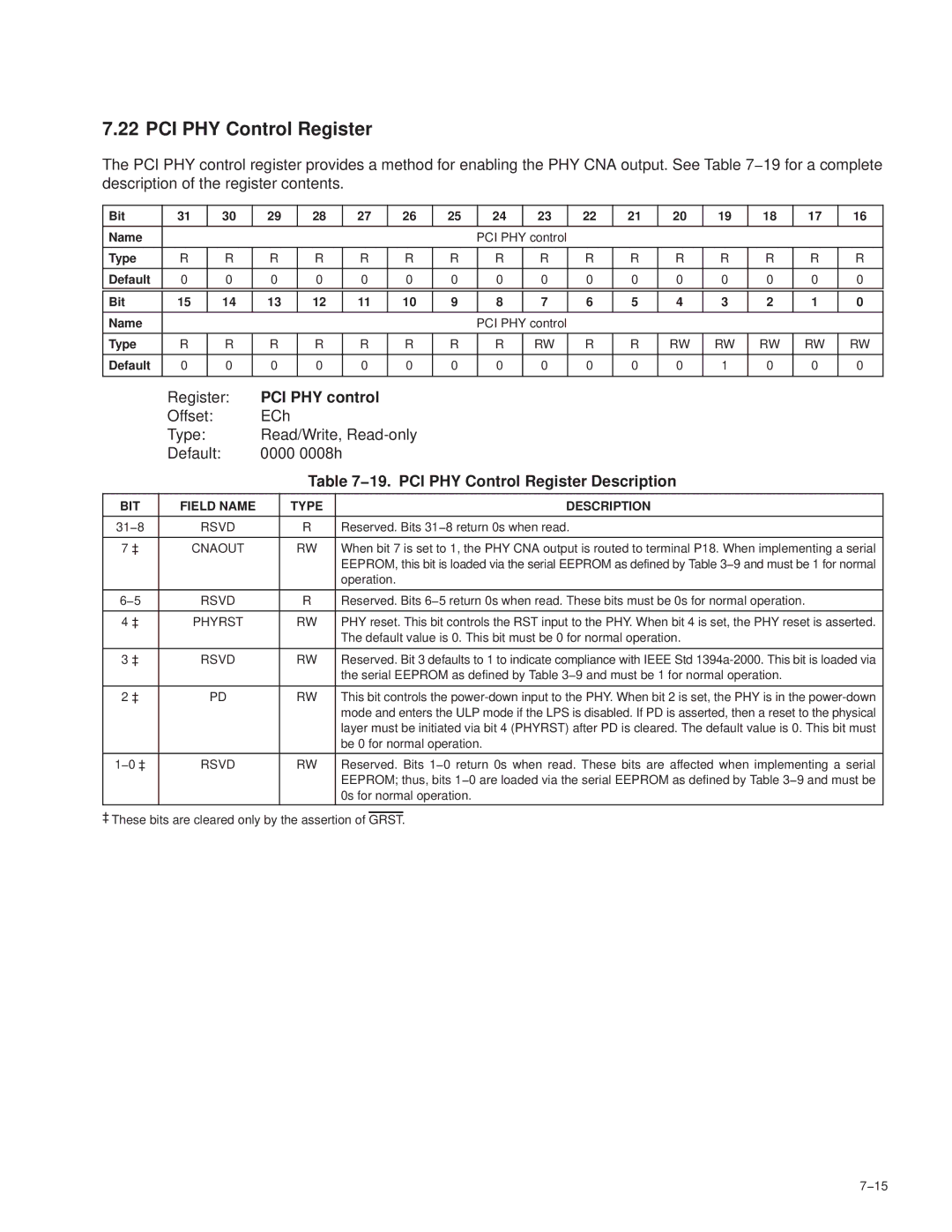
PCI PHY Control Register
PCI PHY control
−19. PCI PHY Control Register Description
PCI miscellaneous configuration
PCI Miscellaneous Configuration Register
−20. PCI Miscellaneous Configuration Register Description
Link enhancement control
Link Enhancement Control Register
−21. Link Enhancement Control Register Description
Subdevid
Subsystem Access Register
Subsystem access
−22. Subsystem Access Register Description
Gpio control
Gpio Control Register
−23. Gpio Control Register Description
= GPIO0
Disablebmc GPIO0
GPIOENB1 GPIO1
GPIODATA1
DMA Context Register Name Abbreviation Offset
−1. Ohci Register Map
Guid ROM Guidrom
Physical request filter low PhysicalRequestFilterLoSet
IsoRecvIntEventClear
Isochronous receive interrupt mask IsoRecvIntMaskSet
PhysicalRequestFilterHiClear
Request Transmit Reserved
Isochronous receive context command
Asynchronous context control ContextControlSet
ContextControlClear
Ohci version
Ohci Version Register
−2. Ohci Version Register Description
RSU
Guid ROM Register
−3. Guid ROM Register Description
Guid ROM
−4. Asynchronous Transmit Retries Register Description
Asynchronous Transmit Retries Register
CSR Data Register
Asynchronous transmit retries
CSR control
CSR Compare Register
CSR Control Register
CSR compare
Bus Identification Register
Configuration ROM Header Register
Configuration ROM header
−6. Configuration ROM Header Register Description
Bus options
Bus Options Register
−7. Bus Options Register Description
Guid low
Guid High Register
Guid Low Register
Guid high
Posted Write Address Low Register
Configuration ROM Mapping Register
Posted write address high
Posted Write Address High Register
−10. Posted Write Address High Register Description
RSU RSC Rscu
Host Controller Control Register
Host controller control
−11. Host Controller Control Register Description
Self-ID buffer pointer
Self-ID Buffer Pointer Register
LPS RSC
Self-ID count
Self-ID Count Register
−12. Self-ID Count Register Description
Isochronous receive channel mask high
Isochronous Receive Channel Mask High Register
Isochronous receive channel mask low
Isochronous Receive Channel Mask Low Register
RSC Rscu
Interrupt Event Register
Interrupt event
−15. Interrupt Event Register Description
Arrq Rscu
Arrs Rscu
−16. Interrupt Mask Register Description
MasterIntEnable
Interrupt Mask Register
Interrupt mask
Arrq RSC
Arrs RSC
Generation
Isochronous transmit interrupt event
Isochronous Transmit Interrupt Event Register
Isochronous transmit interrupt mask
Isochronous Transmit Interrupt Mask Register
Isochronous Receive Interrupt Event Register
Reserved. Bits 31−4 return 0s when read
Isochronous receive interrupt event
Initial bandwidth available
Isochronous Receive Interrupt Mask Register
Initial Bandwidth Available Register
Isochronous receive interrupt mask
Initial Channels Available Low Register
Initial Channels Available High Register
Value for this field is 00h
Fairness Control Register
Fairness control
−22. Fairness Control Register Description
Link control
Link Control Register
−23. Link Control Register Description
Node identification
Node Identification Register
−24. Node Identification Register Description
PHY layer control
PHY Layer Control Register
−25. PHY Control Register Description
Isochronous cycle timer
Isochronous Cycle Timer Register
−26. Isochronous Cycle Timer Register Description
Asynchronous request filter high
Asynchronous Request Filter High Register
−27. Asynchronous Request Filter High Register Description
From that node are accepted
Asynchronous request filter low
Asynchronous Request Filter Low Register
−28. Asynchronous Request Filter Low Register Description
PhysReqAllBusses
Physical Request Filter High Register
Physical request filter high
−29. Physical Request Filter High Register Description
That node are handled through the physical request context
−30. Physical Request Filter Low Register Description
Physical Request Filter Low Register
Physical Upper Bound Register Optional Register
Physical request filter low
Rscu RSU
Asynchronous Context Control Register
Asynchronous context control
−31. Asynchronous Context Control Register Description
Asynchronous context command pointer
Asynchronous Context Command Pointer Register
DescriptorAddress
Isochronous transmit context control
Isochronous Transmit Context Control Register
RSC RSU
Isochronous receive context control
Isochronous Transmit Context Command Pointer Register
Isochronous transmit context command pointer
Isochronous Receive Context Control Register
Context match register see .46 is ignored
When software clears bit 15 run
Not be changed while bit 10 active or bit 15 run is set to
MultiChanMode
−43
Isochronous Receive Context Command Pointer Register
Isochronous receive context command pointer
Isochronous receive context command pointer
Isochronous receive context match
Isochronous Receive Context Match Register
−35. Isochronous Receive Context Match Register Description
Link Enhancement Control Clear A8Ch
DV and MPEG2 Timestamp Enhancements
−1. TI Extension Register Map
Link Enhancement Control Set
Isochronous Receive Digital Video Enhancements Register
Isochronous Receive Digital Video Enhancements
Isochronous receive digital video enhancements
Ohci offset 420h/424h see .44 is cleared to
Reserved. Bits 7 and 6 return 0s when read
420h/424h see .44 is cleared to
CIPStrip1
−3. Link Enhancement Register Description
Reserved. Bit 11 returns 0 when read 10 ‡
Link Enhancement Register
Link enhancement
Timestamp offset
Timestamp Offset Register
−4. Timestamp Offset Register Description
Page
RHB IBR
−1. Base Register Configuration
Base Registers
Address BIT Position
Field Size Type Description
−2. Base Register Field Descriptions
RHB
Is unaffected by bus reset
Long bus reset being performed
LLC to service the interrupt
Timeout
BIT Position Address
−3. Page 0 Port Status Register Configuration
Port Status Register
−4. Page 0 Port Status Register Field Descriptions
−6. Page 1 Vendor ID Register Field Descriptions
−5. Page 1 Vendor ID Register Configuration
Hardware reset and is unaffected by bus reset
Vendor Identification Register
NPA
−7. Page 7 Vendor-Dependent Register Configuration
Vendor-Dependent Register
−8. Page 7 Vendor-Dependent Register Field Descriptions
PC0-PC2 Description
Power-Class Programming
−9. Power Class Descriptions
Node does not need power and does not repeat power
10−8
Flash Media Controller Programming Model
−1. Function 3 Configuration Register Map
11−2
Stepenb
Pcispeed Devsel
Storage controller
Programming interface. This field returns 00h when read
Is deasserted
Flash media base address
Flash Media Base Address Register
−7. Flash Media Base Address Register Description
Capabilities pointer
Subsystem Vendor Identification Register
Capabilities Pointer Register
Subsystem vendor identification
Intsel Bits Useinta Intpin
−8. PCI Interrupt Pin Register
11−8
Maximum Latency Register
Minimum Grant Register
This field returns 00h when read
−12. Power Management Capabilities Register Description
PME Rsvd
Power Management Bridge Support Extension Register
Pmestat RCU
Pmeen
Power management data
Power Management Data Register
−14. General Control Register
SubsystemVendorID
−15. Subsystem Access Register Description
Register at PCI offset 2Ch 11−14
Plln
−16. Diagnostic Register Description
Diagnostic
Tbdctrl
11−16
Slot information
−1. Function 4 Configuration Register Map
Maximum current
12−2
Bit 3 returns 0 when read
Therefore, bit 9 returns 0 when read
Bit 5 returns 0 when read
Transactions therefore, bit 4 returns 0 when read
Syserr RCU
DMA capabilities
Peripheral
12−5
Read
Memory-read line, and memory-read multiple transactions
12−6
Type
SD Host Base Address Register
SD host base address
−7. SD host Base Address Register Description
12−8
12.12 Interrupt Line Register
Space see Section 12−9
Numberslots
Slot Information Register
Register Maximum latency
−11. Maximum Latency Register Description
12−11
Revision 12−12
−13. Power Management Capabilities Register Description
Driver is able to use it
Controller to generate PME
12−13
Power management bridge support extension
Enable. Enables Signaling
Register
Dmasupport bit of each SD host socket is
−15. General Control Register
01 = Intb 10 = Intc 11 = Intd
Dmaen
Register at PCI offset 2Ch
−16. Subsystem Access Register Description
−17. Diagnostic Register Description
Reserved. Bits 31−17 return 0s when read
Slot 1 3.3-V Maximum Current Register
Slot 0 3.3-V Maximum Current Register
Slot 2 3.3-V Maximum Current Register
Slot 4 3.3-V Maximum Current Register
Slot 3 3.3-V Maximum Current Register
Slot 5 3.3-V Maximum Current Register
12−18
1Ch−28h
−1. Function 5 Configuration Register Map
60h−FCh
13−2
Seren
Intdis
13−4
Is enabled and the Smart Card controller has
Tabtsig RCU
Intstat
Offset 08h Type Read-only Default 0780 0000h
Smart Card base address register
Smart Card Base Address Register
Smart Card base address register
Card is a multifunction device
Smart Card base address register 1−4
Smart Card Base Address Register 1−4
13−7
13−8
13.13 Interrupt Line Register
−8. Minimum Grant Register Description
−7. PCI Interrupt Pin Register
Space see Section 13−9
13−10
−9. Maximum Latency Register Description
PMED1 PMED0 D2SUPPORT
−11. Power Management Capabilities Register Description
PMED3HOT
PMED2
Dstate
PME Grst Rsvd
13−12
−13. General Control Register
Gated to reduce power consumption
Pin = 01 = Intb pin = 10 = Intc pin = 11 = Intd pin =
−14. Subsystem ID Alias Register Description
Subsystem ID Alias Register
Class Code Alias Register
Subsystem ID alias
13−15
Smart Card Configuration 1 Register
Smart Card configuration
Smart Card configuration
−15. Smart Card Configuration 1 Register Description
Reserved. Bits 7−0 return 0s when read 13−17
Smart Card Configuration 2 Register
−16. Smart Card Configuration 2 Register Description
Pwrupdelay
13−18
Avdd VCC VDPLL15 VDPLL33 Vccp
Absolute Maximum Ratings Over Operating Temperature Ranges†
Recommended Operating Conditions see Note
Operation MIN NOM MAX Unit
Recommended Operating Conditions
TJ#
Parameter Terminals Operation Test Conditions MIN MAX Unit
Parameter Test Condition MIN MAX Unit
14.4.1 Device
14.4.2 Driver
14.4.3 Receiver
Parameter Test Conditions MIN TYP MAX Unit
Switching Characteristics for PHY Port Interface
Operating, Timing, and Switching Characteristics
Parameter Alternate Test Conditions MIN MAX Unit
Mechanical Information
15−2
Package Option Addendum