Xilinx ML310 manual Gpio LEDs and LCD, Parallel Cable IV Interface

Page 30

R

Chapter 2: ML310 Embedded Development Platform

Parallel Cable IV Interface

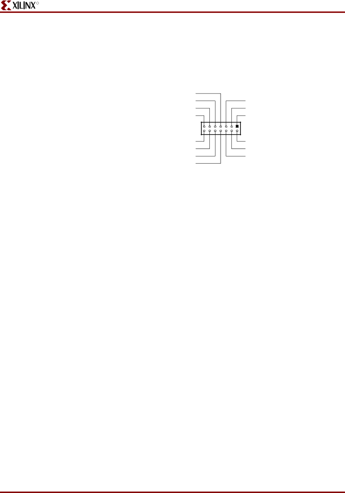
The Parallel Cable IV (PC IV) download cable can also be used to program the XC2VP30. The pinout provided in Figure 2-7is compatible with the PC IV JTAG programming solution.

Figure 2-7shows the pinout of the PC IV JTAG connector.

GND

GND

GND

GND

13

14

NC

NC

PC4_TDI

SYSACE_TSTTDO

GND

GND

GND

1

2

VCCV3

PC4_TMS

PC4_TCK

UG000_05_21_082802

Figure 2-7:PC4 IV JTAG Connector Pinout

System ACE JTAG Configuration Interface

The JTAG Configuration port on the System ACE device is connected directly to the JTAG interface of the XC2VP30 device.Table 2-5shows the JTAG connections from System ACE to the XC2VP30.

Table 2-5:JTAG Connection from System ACE to XC2VP30

Pin Name


System ACE (U38)

XC2VP30 (U37)


FPGA_TCK

80


G7


FPGA_TDO

81


F5


FPGA_TDI

82


F26


FPGA_TMS

85


H8


GPIO LEDs and LCD

GPIO

The ML310 Hardware Platform provides direct GPIO access to eight LEDs for general purpose use and provides indirect access to a 16 pin connector (J13) used to interface the ML310 with a 2 Line by 16 character LCD Display, AND491GST. Access to the GPIO lines is handled by a simple register interface that is connected XC2VP30 GPIO signals.

Figure 2-8shows the connectivity of the ML310 LEDs and LCD.

The user also has an indirect access path to more GPIO capability via PCI Bus accesses when controlling the GPIO header (J5) connected to the ALi M1535D+ South Bridge. Please refer to section “ALi South Bridge Interface, M1535D+, U15” for more details on programming and controlling the ALi M1535D+ GPIO port.

30

www.xilinx.com

ML310 User Guide


1-800-255-7778

UG068 (v1.01) August 25, 2004

Image 30
Contents ML310 User Guide UG068 v1.01 August 25ML310 User Guide ML310 User Guide UG068 v1.01 August 25 Version RevisionUG068 v1.01 August 25 Table of Contents UG068 v1.01 August 25 Manual Contents Additional ResourcesConventions TypographicalOnline Document HandbookChapter Summary of Virtex-II Pro Features Virtex-II ProPowerPC 405 Core RocketIO 3.125 Gb/s TransceiversVirtex-II Fpga Fabric Virtex-II ProDesign Entry Foundation FeaturesFoundation ISE Introduction to Virtex-II Pro, ISE, and EDKImplementation and Configuration SynthesisFoundation ISE Embedded Development Kit Board Level IntegrationML310 Embedded Development Platform OverviewML310 Embedded Development Platform ML310 BoardFeatures OverviewBoard Hardware Clock GenerationDDR Memory Board HardwareDDR Signaling DDR Memory ExpansionU37 DDRA2 DDRDQS02 DDRDQ31 Introduction to Serial Ports Signaling Standards of RS-232Serial Port Fpga Uart RS-232 on the ML310System ACE CF Controller Board Bring-UpNon-Volatile Storage XC2VP30 ConnectivityJtag Connection to XC2VP30 6JTAG Connections to the XC2VP30 and System ACESystem ACE Jtag Configuration Interface Gpio LEDs and LCDParallel Cable IV Interface 8LEDs and LCD Connectivity Gpio LCD Interface UCF Signal Name Translator U37 J13 U35Gpio LED Interface U37 Name U36CPU Debug and CPU Trace CPU Debug DescriptionBuffer U33 J13 9Combined Trace/Debug Connector Pinout CPU Debug Connector Pinout PCI BusCPU Debug Connection to XC2VP30 ML310 Embedded Development Platform 11 PCI Bus and Device Connectivity Pciinta Pciintb Pciintc Pcipar Pcippar Pcirstn Pciprstn Device Name Bus ALi South Bridge Interface, M1535D+, U15113.3V Primary PCI Bus Information Device Vendor 125.0V Secondary PCI Bus Information Device Name VendorParallel Port Interface, connector assembly P1 12ALi South Bridge Interface, M1535D+, U15Serial Port Interface, connector assembly P1 USB, connector assembly J3 IDE, connectors J15 and J16 GPIO, connector J5 System Management Bus SMBus17Type of Gpio Available on Header J5 ALi Gpio Types Number 19Audio Jacks, J1 and J2 Signal name Description AC97 AudioPS/2 Keyboard/Mouse Interface, connector P2 Flash ROM, U4Intel GD82559, U11, 10/100 Ethernet Controller Intel GD82559 Ethernet ControllerIntroduction to IIC/SMBus IIC/SMBus SignalingIIC/SMBus Interface IIC/SMBus on ML310 Board22shows the Fpga connections to all SMBus and IIC devices 14SMBus and IIC Block Diagram SPI Signaling Serial Peripheral Interface SPIPush Buttons, Switches, Front Panel Interface and Jumpers SPI AddressingPush Buttons System ACE Configuration Dipswitch, SW3 CPU Reset, SW2Front Panel Interface Connector, J23 16SW3 SysACE CFG Switch DetailSYACECFGA0 Jumpers Voltage JumperJ10 J11 Coupling ATX Power Distribution and Voltage Regulation MGT Bref Clock Selection Jumpers, J20 and J2117ATX Power Distribution and Voltage Regulation 18Voltage Monitor High-Speed I/O High-Speed I/OML310 PM Connectors 19Personality Module Connected to ML310 BoardPM1 Connector PM2 ConnectorML310 PM Utility Pins Adapter Board PM ConnectorsContact Order PM2 Power and Ground ML310 PM User I/O PinsPM1 Power and Ground PM1 User I/ORXPPAD4 RXPPAD4A25 31 PM1 Pinout ML310 PM2 User I/O RXPPAD21 RXPPAD21AK2532 PM2 Pinout AA5